Wake-on-Shake Hookup Guide
Hardware Overview
Basic Operation
The Wake-on-Shake has a rather simple concept of operation. Once a power supply is connected, as well as a load circuit, the Wake-on-Shake will wake up upon being bumped, touched, or moved, power up the load circuit for 5 seconds, and then return to an inert state.
The sensitivity of bumps or movement can be changed over the serial connection. The user also has the option to increase or decrease the delay time for powering the load circuit.
Power Connections
The Wake-on-Shake has a very low power consumption of <2uA at 3.7V. However, the board itself can be powered with 2.0-5V. There are two different options available for powering the Wake-on-Shake.
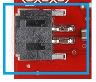
- JST Connector - The JST connector on-board is designed to interface with any single cell lipo batteries available from SparkFun. These will power your Wake-on-Shake at 3.7V.
Alternatively, you can also use the JST Jumper Wire Assembly to connect your project to a power source.
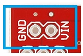
- Power Input Headers - The second option for powering your Wake-on-Shake is through the VIN/GND pins broken out on the top of the board. You will need to solder either bare wires or headers to these pins in order to hook up a power supply to your board through these.
ICSP Header
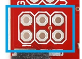
The ISP header on-board follows the standard 6-pin AVR programming header. This gives the user access to reprogram the ATTiny2313A. However, the Wake-on-Shake can be used to its full potential without reprogramming. This is an advanced feature.
Keep in mind that there is no bootloader on this device. You can use any standard 6-pin AVR programmer to upload code via this header. Depending on the type of programmer you are using, you may need to solder either male or female headers onto these pins.
Serial Connection Header
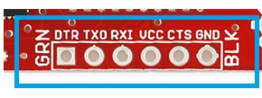
The serial connection header has the standard mating footprint for any 3.3V FTDI Breakout board or FTDI USB-to-Serial cable. For our example, we will be using the breakout board. You can use other materials for serial communication with the Wake-on-Shake, but keep in mind that they should run at 3.3V logic levels.
This header also allows you to access the ADXL362 onboard directly, as well as the EEPROM storage for the ATTIny2313A.
While it is possible to connect the load to the serial port for power, it is possible to draw too much current through these pins. That can lead to damage to the ATTiny2313A, and should be avoided if possible.
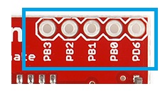
General I/O Pins
The general I/O pins broken out on the Wake-on-Shake can be read for information on their statuses, by default. Serial commands exist to read and write the status of these pins.
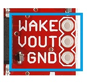
Load Connection Pins
The load connection pins are the main connection point for the rest of your project.
WAKE - The WAKE pin determines the functionality of the pass transistor on the Wake-on-Shake. When held above ~2.7V, the transistor will remain on until released. This allows the load to gate its own power for as long as needed. In other words, this gives the load the power to control when its power is disconnected.
VOUT - This is power output for the rest of your circuit. Output is dependent on the supply input for the Wake-on-Shake.
GND - The name says it all! This is your ground connection for your load circuit.
Onboard ICs
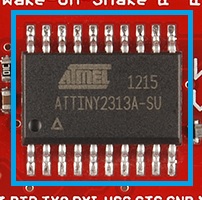
- ATTiny2313A
The microcontroller driving the Wake-on-Shake is the ATTiny2313A. This is a small 20-pin IC with low-power consumption. Even in active mode, this IC only pulls 190uA, and draws as little as 24uA in idle mode.
This IC holds the main code driving the Wake-on-Shake, and can be reprogrammed over the serial connection header.
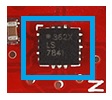
- ADXL362
The accelerometer onboard that watches for bumps, knocks, or other movement triggers for the Wake-on-Shake is the ADXL362. The 3-axis accelerometer can measure 2g, 4g or 8g ranges. It has a high resolution of 1 mg/LSB at +/- 2g, and interfaces over an SPI connection.
This accelerometer draws very little power, only 3uA at 400Hz, 270 nA when in motion-triggered wake-up mode, and down to 10nA in standby mode.
