TSH82 Configurable OpAmp Hookup Guide
 Pete-O
Hardware Overview
The TSH82 Configurable OpAmp Board is meant to be hacked on, so you'll want to be familiar with the sections of the circuitry.
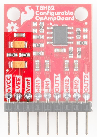
On the far left side of the board is the power and reference section, the middle section covers stage 1 of the amplifier, and the far right side has stage 2. Each section also has three corresponding pins directly below in the picture.
Power and Reference
Positive voltage goes into +VCC, and negative voltage (or ground) goes into -VEE. The board generates an onboard reference voltage by way of two 2.2k 1% resistors decoupled with 10.1uF, giving a value halfway between +VCC and -VEE with a low frequency cutoff of about 15Hz. If you need better performance, VREF is accessible from the header and can be driven to any voltage between +VCC and -VEE without damaging the board.
Stages One and Two
Electrically speaking, the stages are identical. The default configuration is inverting with a gain of -4.7 with a bandwidth of almost 10MHz. Signal input is on -IN1 and output is taken from OUT1 (or -IN2 and OUT2 for stage two). Input signals are AC coupled with 1.0uF caps, and the input impedance is 10K with a low frequency cutoff of 15.9Hz. Outputs are DC coupled, so don't forget to add a capacitor to the output if you're running a single-ended supply and need to strip out the DC component. Of course, this isn't an issue if you're running the output of stage 1 to the input of stage 2.
 |
 |
| Stage 1 | Stage 2 |
All Those Jumpers
On the back of the board you'll find 10 solder jumpers that can be used to change the board's performance, but nothing there needs to be changed to use it in it's default state. To demonstrate how to use the jumpers, we'll first describe their functions, then show you different circuit configurations with corresponding jumper settings. For the sake of clarity, it might be a good idea to have the schematic open for reference as you read through the jumper settings description.
Stage 1:
 |
 |
| Stage 1 | Stage 1 Schematic |
Stage 2:
 |
 |
| Stage 2 | Stage 2 Schematic |
Input signal path:
- JP1 and JP2 - 3 way solder jumpers used to change the input signal path in Stage 1.
- JP1 - inverting input
- JP2 - non-inverting input
- JP3 and JP4 - 3 way solder jumpers used to change the input signal path in Stage 2.
- JP3 - inverting input
- JP4 - non-inverting input
There are small traces within these jumpers to set the default inverting configuration that will have to be cut out if you wish to change to differential or non-inverting configurations.
AC vs DC coupling
- JP5 and JP6 - Solder jumper used to select between AC and DC coupling for the inputs to Stage 1.
- JP5 - inverting input
- JP6 - non-inverting input
- JP7 and JP8 - Solder jumper used to select between AC and DC coupling for the inputs to Stage 2.
- JP7 - inverting input
- JP8 - non-inverting input
Vref
- JP9 - allows the user to tie the non-inverting input of stage 1 to Vref through a 47k resistor for differential operations.
- JP10 - same functionality as JP9 but for stage 2
As you can see, there are a lot of options. But if any of that leaves you confused, let us show you some workable configurations!