TSH82 Configurable OpAmp Hookup Guide
 Pete-O
Configurations
Inverting, Gain = -4.7, AC-coupled Input, 0-10V Supply (Default)
This is the easiest configuration to use as it requires no changes to the jumpers on the board.
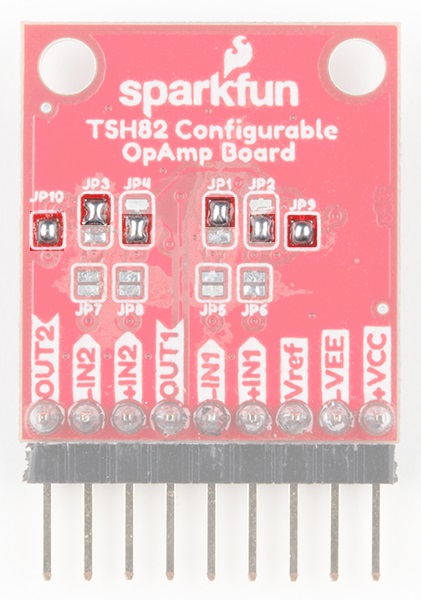
In the picture below, the jumper settings for this default mode are highlighted for your reference. Note the small traces bridging the pads of the solder jumpers. If the board does not perform as expected, double check that these traces are still present. If they're not, just replace them with a blob of solder to make the default connections as shown here.
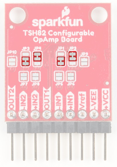
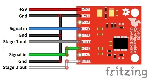
+10VDC power input is on +VCC and ground is on -VEE. Vref will assume a value near +5V.
For stage 1, signal input is between -IN1 and -VEE, and output is taken between OUT1 and -VEE. It's effectively the same for stage 2: signal input is between -IN2 and -VEE, and output is taken between OUT2 and -VEE. Each stage will give you a gain of -4.7, so to keep the output in the linear region your input signal can't be more than 2.12Vpp, as calculated here:

If you're running both stages in sequence, that maximum becomes 453mVpp. If you're not sure what your input signal magnitude is going to be, it's probably a good idea to use a potentiometer at the input of your circuit.
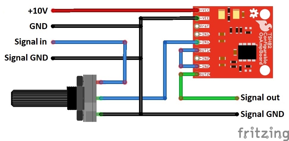
Differential Input, Gain = 4.7, DC-coupled Input, 0-5V Supply
Differential configuration gives the user the ability to compare two dynamic voltages rather than comparing one against a static reference. The jumper settings for differential configuration are as shown below.
The picture above shows both stages set up for differential operation with DC input coupling (jumpers 5-8 are set). Put your first signal input, V1, between +IN1 and ground, and put your second signal input, V2, between -IN1 and ground. +5V goes in on +VCC and ground goes to -VEE. Also, set Vref to 0V by connecting the Vref header pin to -VEE. Gain for the circuit is 4.7, as calculated here:

And, of course, all of this also applies to stage 2, just transpose all the numbers in the pin names from 1's to 2's.
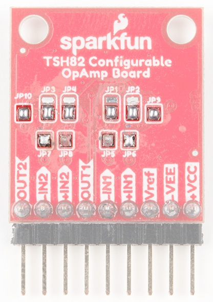
Non-inverting, Gain = 4.7, AC-coupled Input, 0-6V Supply
While the classic non-inverting topology can’t be realized without replacing parts on the board, non-inverting functionality can be achieved by starting with the differential configuration and tying the inverting input to Vref. The jumper settings can be seen below.
The circuit is fully functional, but it's got a couple of quirks that the user should be aware of before use. First, because this isn't the "normal" non-inverting circuit topology, gain is about 4.7 instead of 5.7. Second, and for the same reason, there's some input offset that you might have to deal with, but it's not complicated. Specifically with this topology, Vref will normally sit halfway between +VCC (6V) and -VEE (0V), but the output will skew somewhat positive, to around 4V without any signal input. As a result, your output swing can only go +/-2V around Vref before it starts to clip, making your maximum allowable input signal about 851mVpp. If those numbers work for your design, then you're good to go!
On the other hand, if you move Vref (covered in the next section) to about 1.6V, the output will come back to 3V and allow the full +/-3V output swing. Dividing by our gain of 4.7 gives us a maximum input signal of 1.28Vpp, which is still less than the 3.6Vpp allowable window created by moving the reference voltage.