SparkPunk Sequencer Theory and Applications Guide
 Byron J.
Theory Of Operations
In order to modify the sequencer, it is useful to understand some of its internal workings. We're going to step through the functional blocks on the schematic, and discuss how each works in more detail. If you'd like a better look at the schematic or PCB artwork, you can download the Eagle files from Github.
The sequencer was designed in simulation before the prototype hardware was constructed. Also in the Github repo are Spice simulation files, which run in the free LTSpice environment. The simulations proved to be very valuable, especially in getting the variable-width gate circuit working.
The SparkPunk Sequencer is a mixed-signal circuit -- it consists of a digital section for the clocking and play logic, and an analog section to generate the control voltage and gate.
Digital Section
We'll start with the digital portions of the circuit. These are mostly implemented using CD4000-series CMOS logic chips. These chips are rated for a wide range of supply voltage -- unlike some newer, more sensitive logic chips, they're prefectly happy being powered by a 9V battery.
Run Button
The RUN pushbutton on the sequencer is a momentary-contact type switch. To use it in a toggling application (push once to turn on, push again to turn off), it's connected to one section of a CD4013 flip-flop. The switch is connected to the clock input on the flip-flop, and the inverted logic output is looped back to the data input.
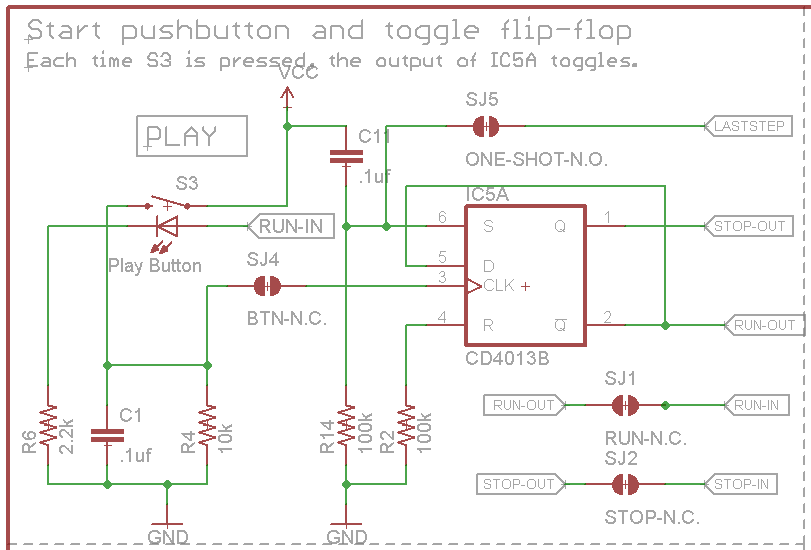
Every time the button is pushed, the flip-flop output changes state.
The flip-flop has two outputs, called Q and Q, and their functions can be described as:
- Q is called "Stop." It is asserted when the sequencer is stopped.
- Q is called "Run." It is asserted when the sequencer is running.
The run and stop signals are used in other portions of the circuit -- other circuitry needs to react appropriately when the sequencer is started or stopped, and these signals allow for those actions.
The flip-flop also has data preset inputs (the Set and Reset pins). When power is applied, the capacitor on the Set input holds it high for a moment, causing the flip-flop to initialize in the Set state, so the sequencer is stopped by default.
The Run signal is connected to the LED in the button, so it illuminates while the sequencer is playing.
Tempo Clock and Divider
The next functional block of the circuit is the tempo clock. It consists of two stages: the clock oscillator, and a divider.
The oscillator portion is is based around a 7555, which is a low-power CMOS version of the venerable 555 timer IC. The basic circuit configures the timer in astable (free-running) mode, with the timing set by a potentiometer.
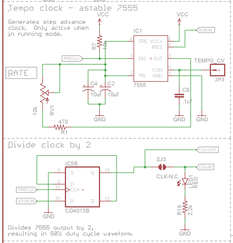
When the sequencer is running, the clock is enabled by the Run signal from the button circuit. The 7555 does not run when the sequencer is stopped.
The output from the 7555 is not used directly by the rest of the sequencer. The 7555 output is further conditioned using a divide-by-two circuit, using the other flip-flop in the CD4013. This is done for several reasons:
- First, the clock generated by the 7555 isn't perfectly symmetrical - the pulse width changes with frequency. This made the short/long switching hard to achieve, and also made the tempo LED hard to discern - wide pulses meant it was almost always illuminated.
- Second, by dividing the clock down, we can achieve a useful range of tempos with smaller timing capacitors. The division in half has the same effect as doubling the capacitor value.
- The divided-down clock has a pulse width of 50%, which is then used as an input to the system the generates the short (half-step long) gates.
- Finally, there was an otherwise unused flip-flop in the CD4013.
The Q output of the flip-flop is the clock signal used by the rest of the circuit. It also drives the RATE indicator LED.
CD4017
The CD4017 is essentially a sequencer on a chip. It's the heart of this kit, and the rest of the circuit serves in a role to support its basic functionality. Internally, it has a binary ripple counter and a demultiplexer. It receives pluses on pin 14, which causes the counter to increment. The value of the counter is decoded so that one of the ten output pins (labeled Q0 through Q9) is active at a time. Each clock pulse causes the next output pin to be selected, and the selection starts over at Q0 after Q9 has been reached.
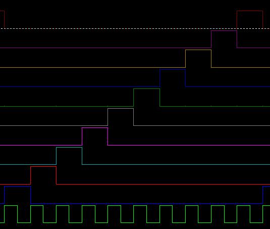
The timing of the CD4017 can be seen in the diagram above. The clock is the bottom trace, and the ten outputs are the traces above that. On each rising edge of the clock, the high logic level progresses to the next successive output.
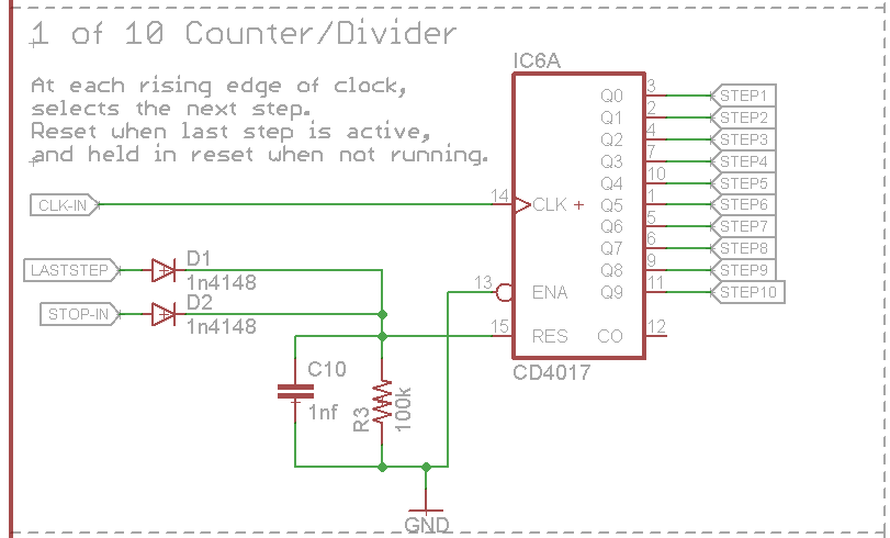
The CD4017 also has a reset pin, which restarts the output selection from Q0 when it is asserted. This allows us to implement some more subtle behavior:
- When the sequencer is not playing, it sits at the first step. This is done by connecting the stop signal to the reset pin on the CD4017.
- When the sequence starts playing, the reset line is held high for a brief moment by capacitor C10. This means that the CD4017 effectively ignores the first clock pulse, and that the sequence starts on the first step. Without this cap, the clock starts as soon as the run button is pressed, and the sequence immediately advances to the second step.
- By feeding the selection pulse from one of the step outputs back to the reset pin, we can constrain the pattern to fewer than ten steps.
Analog Circuitry
The Steps
The ten outputs from the CD4017 are fed to the ten step circuits. Each step is a copy of the same circuit.
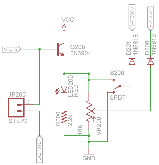
The CD4017 outputs are only rated to supply a couple of milliamps, so the step circuit starts with a transistor configured as an emitter follower, allowing for more output current to illuminate the LED. The step selection voltage is also fed to the slider, which is wired as a voltage divider. When the step is selected, the wiper of the slider travels between ground and about 8.3V. The gate switch on each step selects between the selection voltage, and ground.
The slider wipers and switches are coupled to common buses, POTSUM and GATESUM respectively, using diodes. This configuration implements the selection of the maximum voltage. Since only one step is selected at a time, that means all but one input to the max function will be zero, allowing the selected step to dominate.
Slider Voltage Processing
To understand how the slider voltage is manipulated, we need to step back and look a little more closely at the device it is feeding. The SparkPunk Sound Generator uses a 7556 dual timer IC as its main tone source. The 7556 has control voltage inputs, but they behave in a somewhat counterintuitive manner -- a higher voltage on the CV pin results in a lower frequency -- an inverse relationship. It also works best in the middle of the range between ground and the power supply voltage -- leaving that range causes the 7556 to stutter or stall.
The LM358 amplifier IC is also constrained. The datasheet states that the maximum input level is 1.5V below the positive supply rail.
The sequencer manages the voltages coming from the slider wipers accordingly, inverting and scaling the voltage into a usable range.
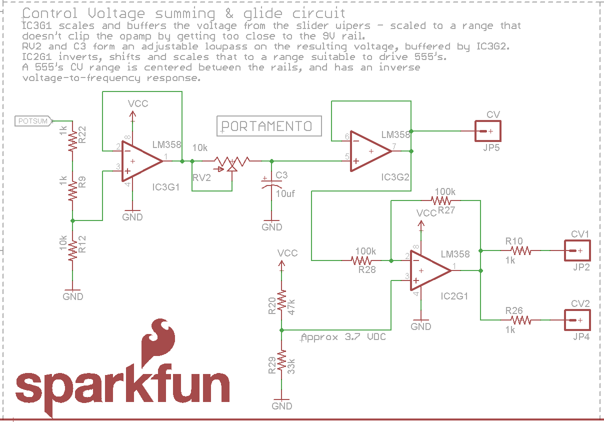
Follwing the signal through the circuit, first we find a divider, to drop the level into the LM358's allowable range. That signal is buffered with an opamp stage, then fed to the variable lowpass filter that implements the slide. As the resistance of RV2 is increased, it takes C3 longer to charge. The filter is buffered with another opamp stage. Finally, the third opamp inverts and offsets the control voltage into a range suitable for the 7556.
Switch Voltage Processing
The gate behavior of the sequencer can be changed between short gates, which are each one-half step in duration, and long gates, which are a complete step long. Additionally, the gate is only driven when the sequencer is running, so it sits quietly when stopped. The logic behind the gate can be expressed by the following equations:
Long gate = running && step switch
Short gate = running && step switch && clock pulse
This logic is implemented using analog processing.
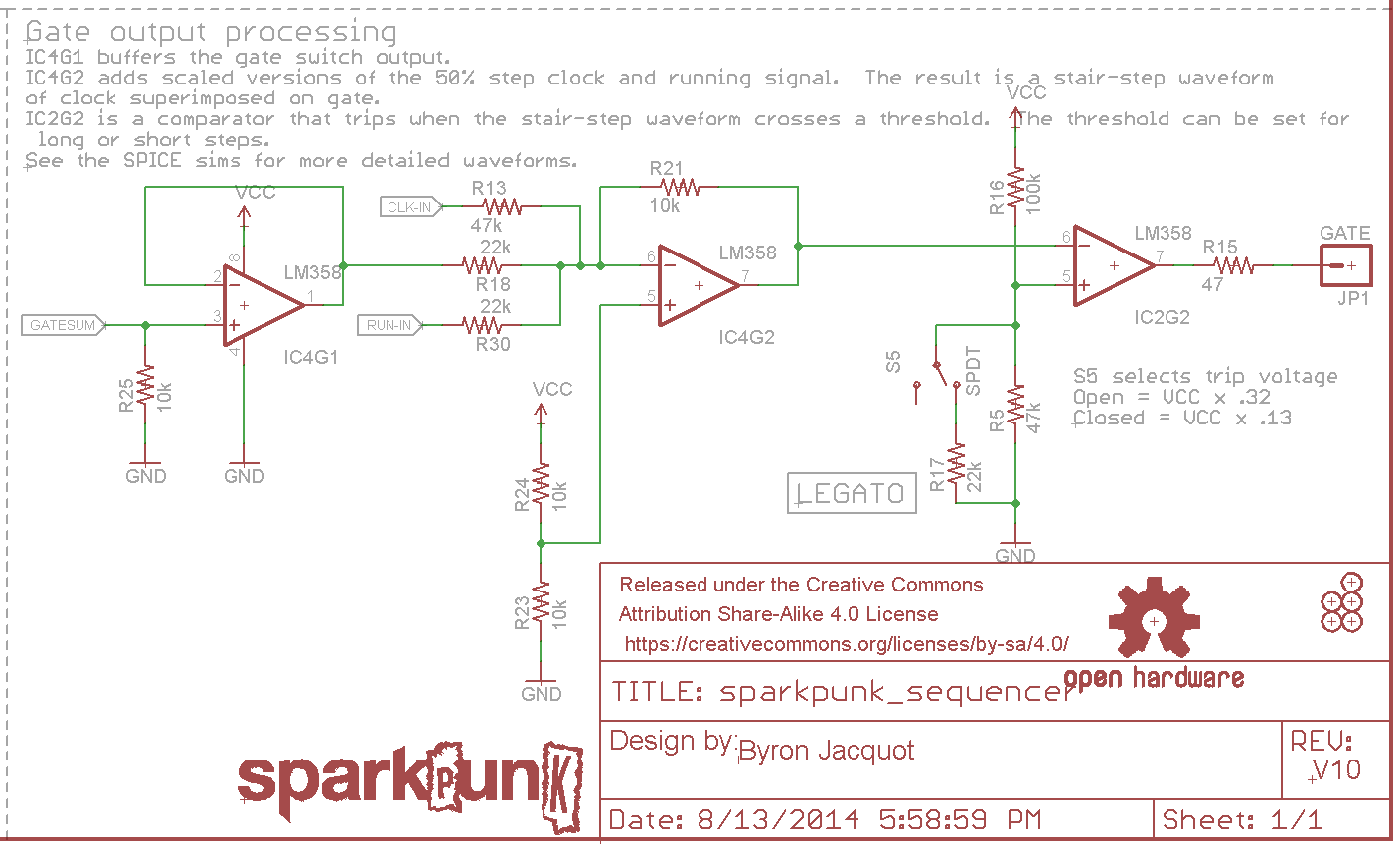
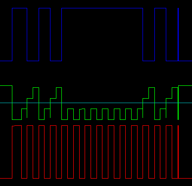
The running, clock, and switch signals are scaled and added together, resulting in a stair-step shaped waveform. Each of those signals contributes a portion to the overall sum, as denoted by the colored rectangles below.

Notice that when a clock pulse overlaps a step switch that is turned on, they add up to the highest step shown, and the step switch by itself is the second highest step. A clock pulse that doesn't overlap the switch being set is lower still. We use an op-amp comparator circuit to apply thresholds to discern those first two stairstep levels.
The actual circuit uses an inverting op-amp stage to do the summing, so the result is upside down compared to that shown above. This is corrected by the comparator stage that generates the gate, which is also inverts.
The threshold voltage on the comparator determines the length of the gate pulses. Short gates are generated when the threshold voltage is tripped by the sum of the clock and switch signals.

The clock is shown in red, and the inverted stairstep waveform in green. The comparator threshold is shown in light blue, superimposed over the stairstep. When the stairstep falls below the threshold, the comparator output, in dark blue, switches high.
Long gates use the same processing, but the threshold voltage is adjusted so that only the switch voltage is required to trip the comparator.
Strong Foundation
With the understanding of the internal details described above, we're how ready to look at some ways that those details can be leveraged into modifications and more sophisticated deployments.