SparkFun MicroMod Input and Display Carrier Board Hookup Guide
 Alex the Giant, Ell C
Hardware Overview
In this section we'll cover the various hardware and sensors included on the MicroMod Input & Display Carrier Board.
Common Components
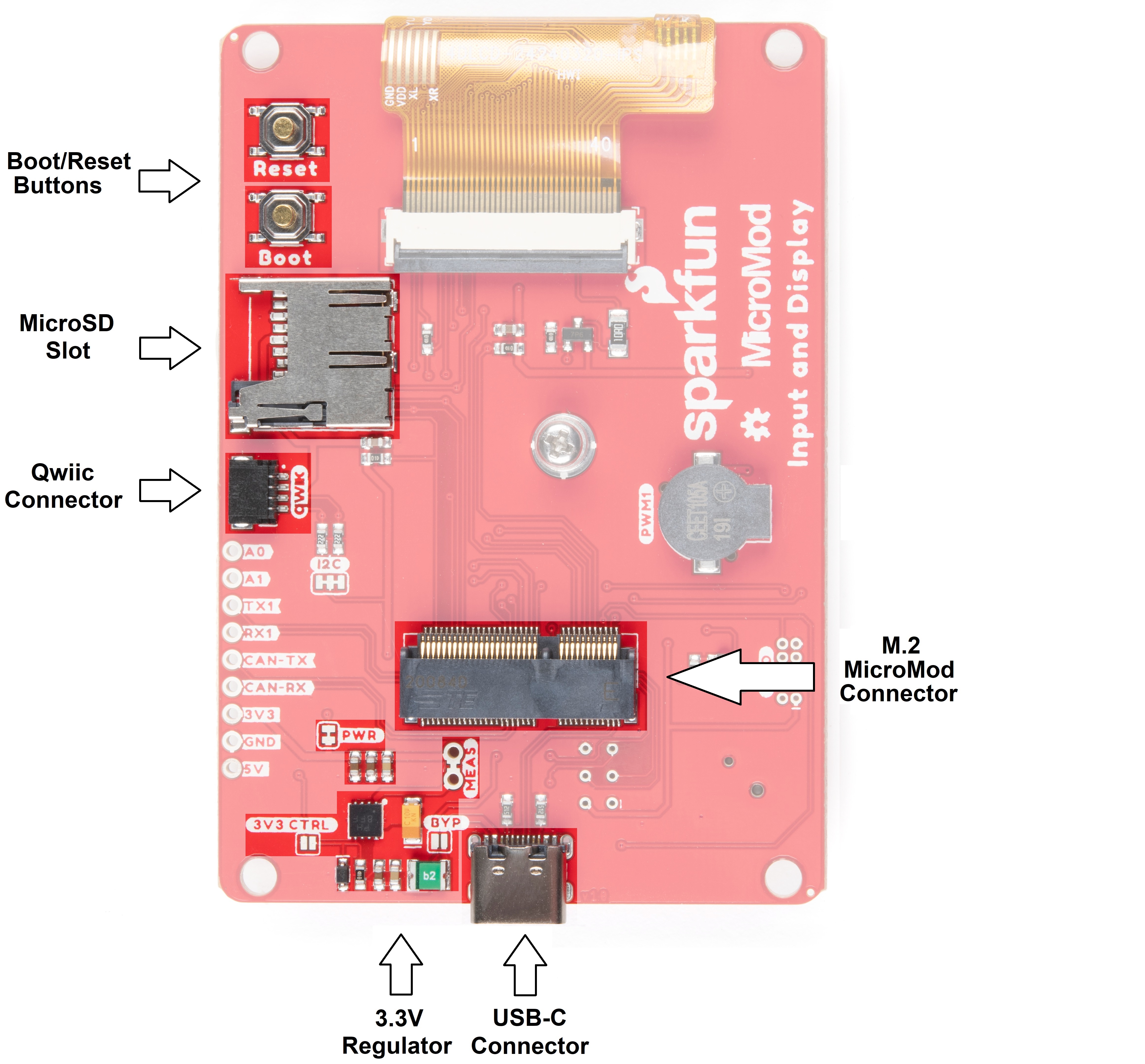
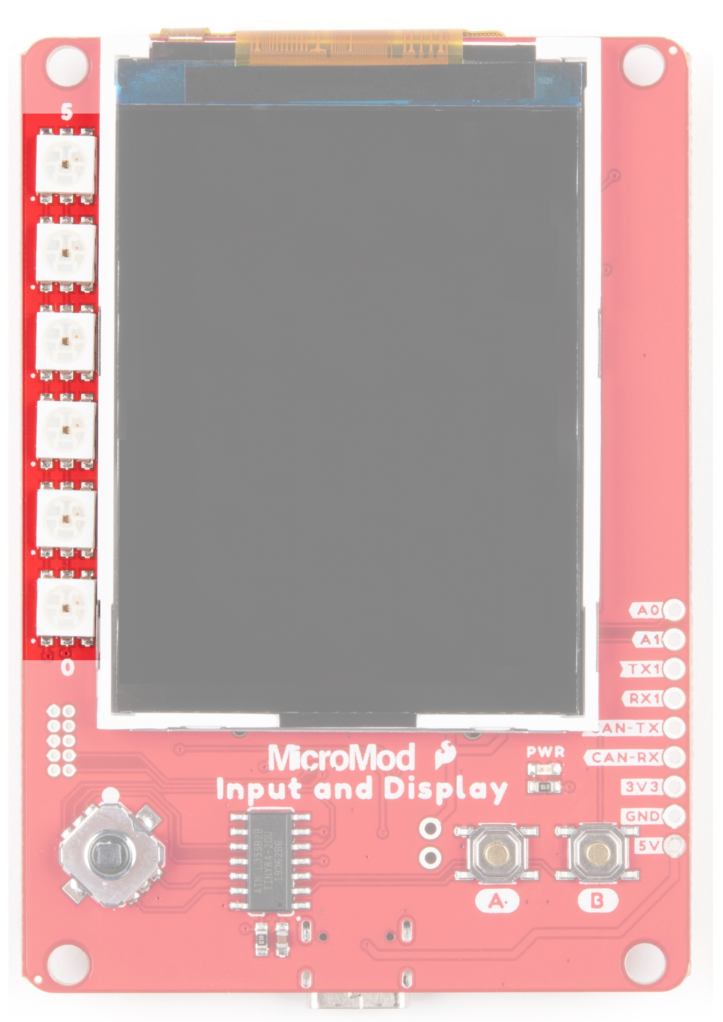
Most SparkFun MicroMod Carriers will have some common components and all MicroMod Carriers will have the keyed M.2 MicroMod Connector to plug your processor into. The photo and list below outline some of the components you can expect on most SparkFun MicroMod Carriers.
- M.2 MicroMod Connector - This special keyed M.2 connector lets you install your MicroMod Processor of choice on your Input & Display Carrier Board.
- USB-C Connector - Connect to your computer to program your Processor and also can provide power to your MicroMod system.
- 3.3V Regulator - Provides a regulated 3.3V and sources up to 1A.
- Qwiic Connector - The standard Qwiic connector so you can add other Qwiic devices to your MicroMod system.
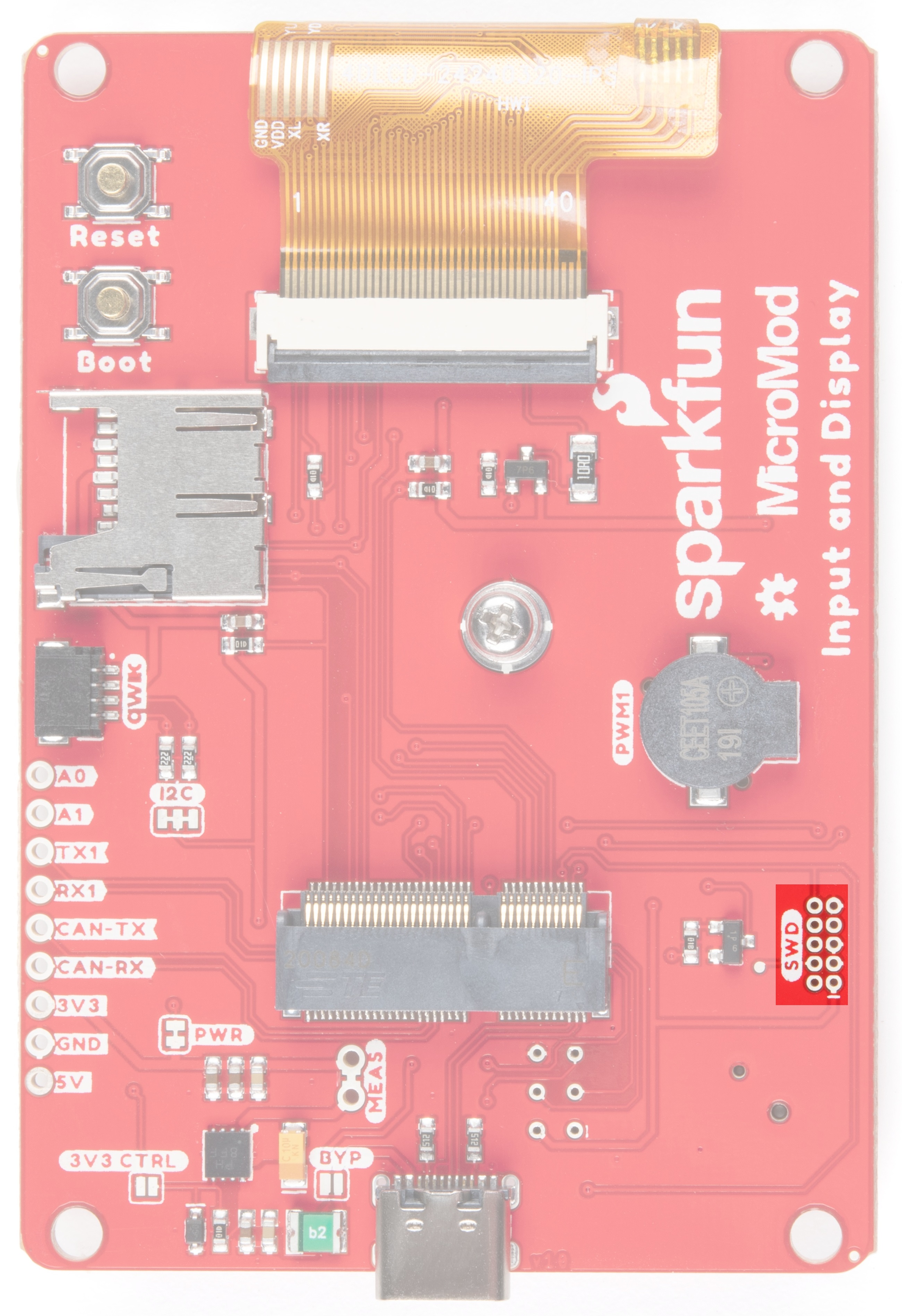
- Boot/Reset Buttons - Push buttons to enter Boot Mode on Processor boards and to Reset your MicroMod circuit. More information needed - LAC
- microSD Slot - Insert a microSD card for reading and writing data.
Power
The Input and Display Carrier Board takes an input voltage range from 2.7V - 6V via the USB-C connector. We've incorporated a power regulation circuit that caps the voltage for power sensitive circuits and the Qwiic connector.
Input & Display Carrier Board Specific Components
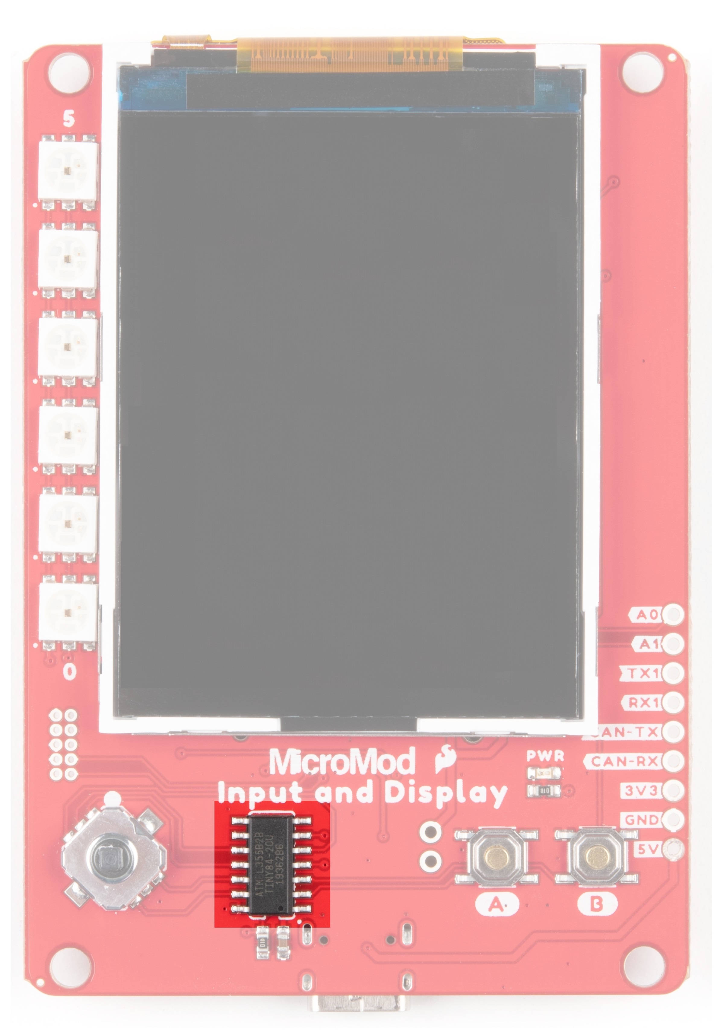
ATTiny84
We've populated this carrier board with Atmel's ATtiny84 with 8kB of programmable flash. This little guy is preprogrammed to communicate with the processor over I2C to read button presses.
TFT Display
4DLCD's 24320240-IPS is a color active matrix LCD module incorporating amorphous silicon TFT (Thin Film Transistor). The module display area measures 2.4" and contains 240 x 320 pixels.
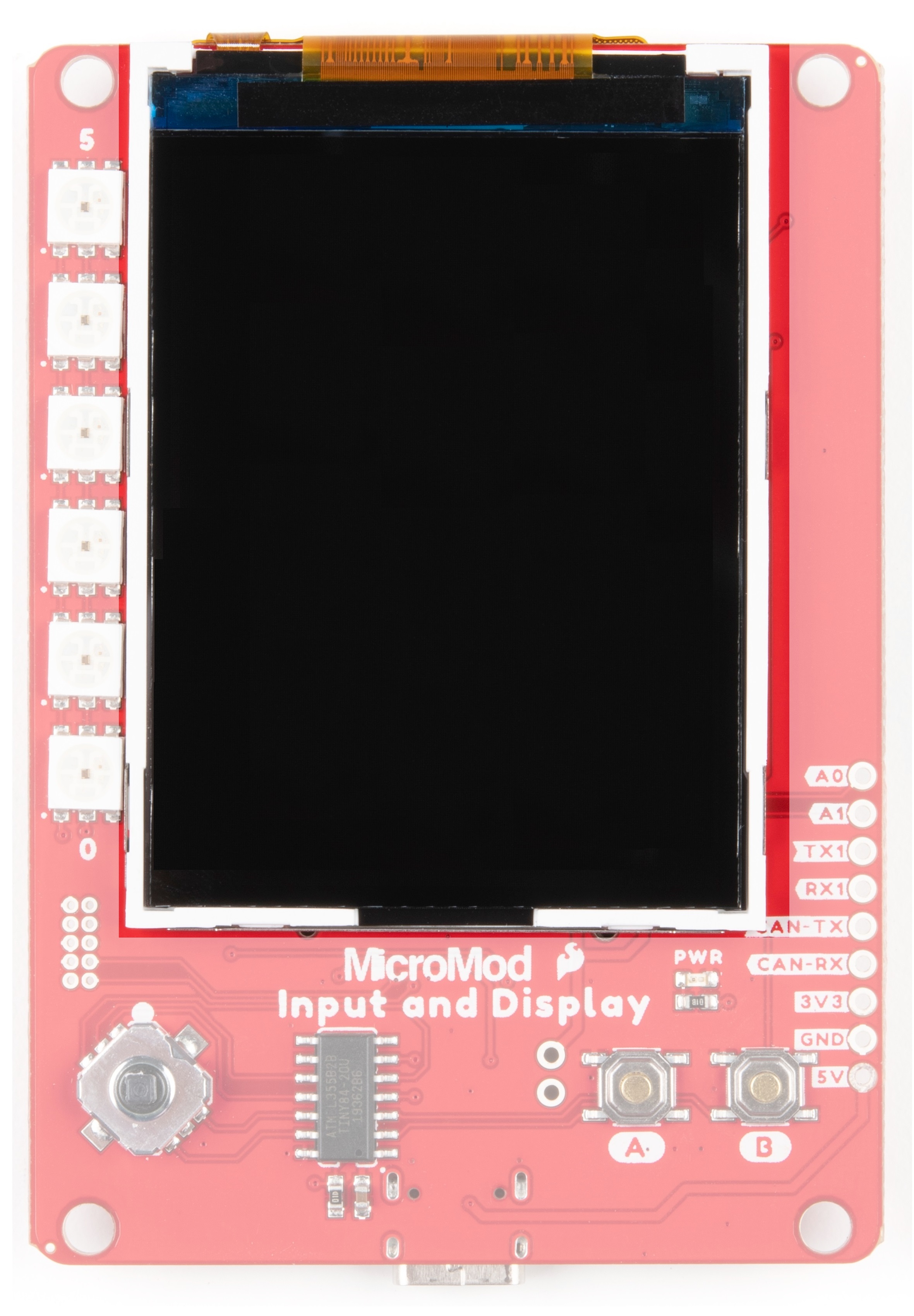
LEDs
The Input and Display Carrier Board has 6 Addressable APA102 LEDs.
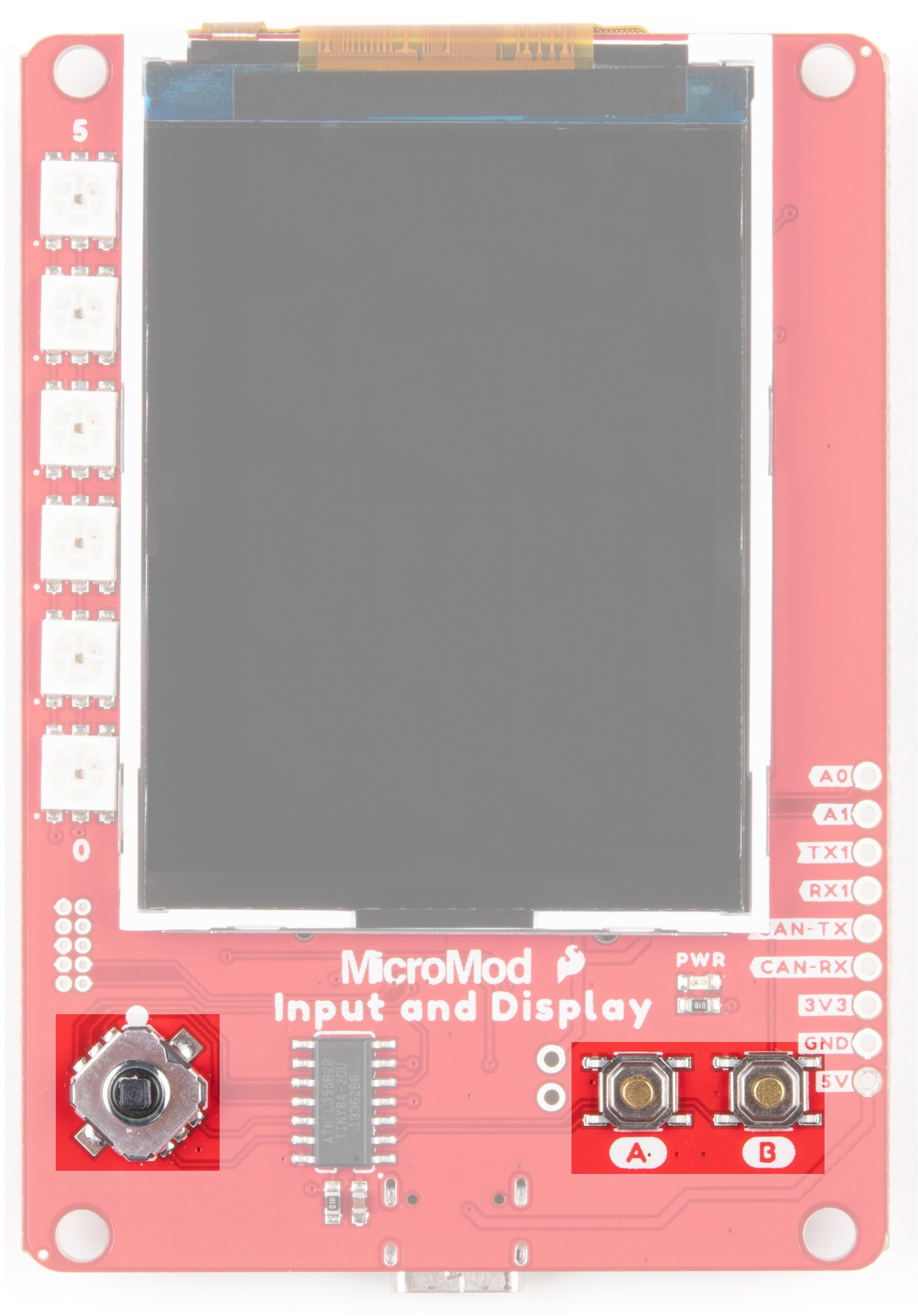
Input Buttons
Button button, who's got the button? We do! We have two input buttons (A and B), and a 5 way switch that allows you to navigate a UI or play an onboard game.
JTAG Debugging
We've populated the JTAG footprint for more advanced users who need breakpoint level debugging. We recommend checking out our JTAG section for the compatible JTAG programmer and debugger.
Jumpers
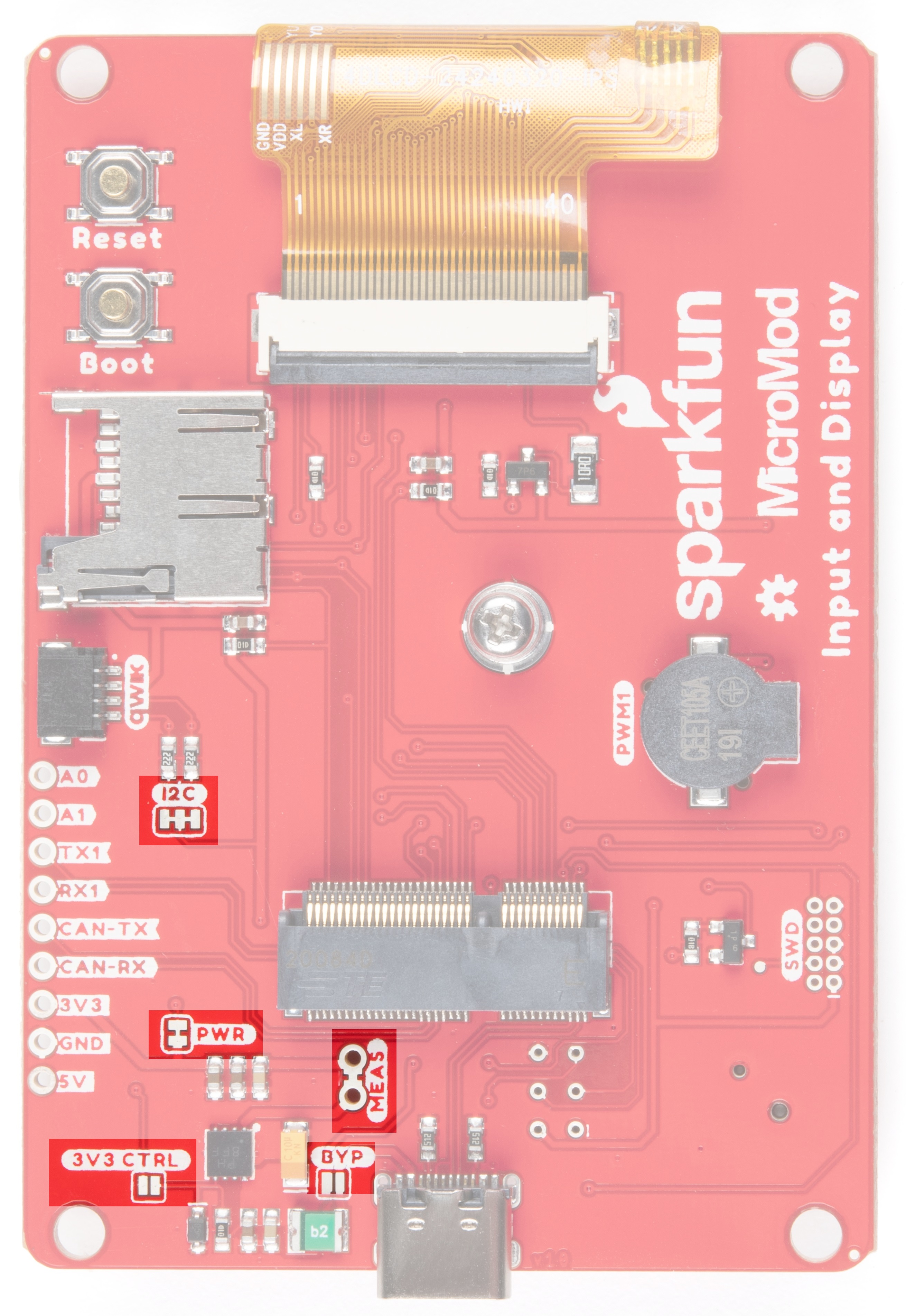
I2C Jumper
If you are daisy-chaining multiple Qwiic devices, you will want to cut this jumper; if multiple sensors are connected to the bus with the pull-up resistors enabled, the parallel equivalent resistance could create too strong of a pull-up for the bus to operate correctly. As a general rule of thumb, disable all but one pair of pull-up resistors if multiple devices are connected to the bus. To disable the pull up resistors, use an X-acto knife to cut the joint between the two jumper pads highlighted below.
PWR Jumper
Cutting this jumper will disable the "Power" LED on the front of the board.
3V3CTRL Jumper
Many of the MicroMod carrier boards have an RTC backup battery on board and as part of the standardized voltage regulation circuit we include a 3V3 jumper that, when closed, allows you to control the 3V3 control regulator. This shuts down everything on the 3V3 rail but the battery keeps the processor awake. The Input and Display Carrier Board does not have a backup battery, so this jumper should remain open.
BYP Jumper
If you really, really, REALLY need more power, closing this jumper will bypass the 2A fuse. Close at your own risk!
Measure Jumper
Want to measure the juice running through your circuits? Cut the trace between these PTH pads in order to measure the current with a Digital MultiMeter.
PinOuts
| AUDIO | UART | GPIO/BUS | I2C | SDIO | SPI | Dedicated |
| Function | Bottom Pin |
Top Pin |
Function | ||||||
|---|---|---|---|---|---|---|---|---|---|
| (Not Connected) | 75 | GND | |||||||
| 3.3V | 74 | 73 | G5 / BUS5 | ||||||
| RTC_3V_BATT | 72 | 71 | G6 / BUS6 | ||||||
| SPI_CS1# | SDIO_DATA3 (I/O) | 70 | 69 | G7 / BUS7 | |||||
| SDIO_DATA2 (I/O) | 68 | 67 | G8 | ||||||
| SDIO_DATA1 (I/O) | 66 | 65 | G9 | ADC_D- | CAM_HSYNC | ||||
| SPI_CIPO1 | SDIO_DATA0 (I/O) | 64 | 63 | G10 | ADC_D+ | CAM_VSYNC | |||
| SPI COPI1 | SDIO_CMD (I/O) | 62 | 61 | SPI_CIPO (I) | |||||
| SPI SCK1 | SDIO_SCK (O) | 60 | 59 | SPI_COPI (O) | LED_DAT | ||||
| AUD_MCLK (O) | 58 | 57 | SPI_SCK (O) | LED_CLK | |||||
| CAM_MCLK | PCM_OUT | I2S_OUT | AUD_OUT | 56 | 55 | SPI_CS# | |||
| CAM_PCLK | PCM_IN | I2S_IN | AUD_IN | 54 | 53 | I2C_SCL1 (I/O) | |||
| PDM_DATA | PCM_SYNC | I2S_WS | AUD_LRCLK | 52 | 51 | I2C_SDA1 (I/O) | |||
| PDM_CLK | PCM_CLK | I2S_SCK | AUD_BCLK | 50 | 49 | BATT_VIN / 3 (I - ADC) (0 to 3.3V) | |||
| G4 / BUS4 | 48 | 47 | PWM1 | ||||||
| G3 / BUS3 | 46 | 45 | GND | ||||||
| G2 / BUS2 | 44 | 43 | CAN_TX | ||||||
| G1 / BUS1 | 42 | 41 | CAN_RX | ||||||
| G0 / BUS0 | 40 | 39 | GND | ||||||
| A1 | 38 | 37 | USBHOST_D- | ||||||
| GND | 36 | 35 | USBHOST_D+ | ||||||
| A0 | 34 | 33 | GND | ||||||
| PWM0 | 32 | 31 | Module Key | ||||||
| Module Key | 30 | 29 | Module Key | ||||||
| Module Key | 28 | 27 | Module Key | ||||||
| Module Key | 26 | 25 | Module Key | ||||||
| Module Key | 24 | 23 | SWDIO | ||||||
| UART_TX2 (O) | 22 | 21 | SWDCK | ||||||
| UART_RX2 (I) | 20 | 19 | UART_RX1 (I) | ||||||
| CAM_TRIG | D1 | 18 | 17 | UART_TX1 (0) | |||||
| I2C_INT# | 16 | 15 | UART_CTS1 (I) | ||||||
| I2C_SCL (I/0) | 14 | 13 | UART_RTS1 (O) | ||||||
| I2C_SDA (I/0) | 12 | 11 | BOOT (I - Open Drain) | ||||||
| D0 | 10 | 9 | USB_VIN | ||||||
| SWO | G11 | 8 | 7 | GND | |||||
| RESET# (I - Open Drain) | 6 | 5 | USB_D- | ||||||
| 3.3V_EN | 4 | 3 | USB_D+ | ||||||
| 3.3V | 2 | 1 | GND | ||||||
| Notes | Primary Function | Bottom Pin | Top Pin | Primary Function | Notes |
|---|---|---|---|---|---|
| 61 | SPI_CIPO | ||||
| 59 | SPI_COPI | ||||
| 57 | SPI_SCK | ||||
| 55 | SPI_CS# | microSD Chipselect# | |||
| 47 | PWM1 | Buzzer | |||
| Display Reset# | G2/BUS2 | 44 | 43 | CAN-TX | |
| APA102 Data | G1 / BUS1 | 42 | 41 | CAN_RX | |
| APA102 Clock | G0 / BUS0 | 40 | 39 | GND | |
| A1 | 38 | ||||
| A0 | 34 | ||||
| Display Backlight# | PWM0 | 32 | |||
| 23 | SWDIO | ||||
| 21 | SWDCK | ||||
| 19 | UART_RX1 | ||||
| Display D/C | D1/CAM_TRIG | 18 | 17 | UART_TX1 | |
| I2C_Interrupt | 16 | ||||
| I2C_SCL | 14 | ||||
| I2C_SDA | 12 | 11 | BOOT | ||
| Display Chipselect# | D0 | 10 | 9 | USB_VIN | |
| 7 | GND | ||||
| RESET | 6 | 5 | USB_D- | ||
| 3.3V_EN | 4 | 3 | USB_D+ | ||
| 3.3V | 2 | 1 | GND |
| Signal Group | Signal | I/O | Description | Voltage | Power | 3.3V | I | 3.3V Source | 3.3V |
|---|---|---|---|---|
| GND | Return current path | 0V | ||
| USB_VIN | I | USB VIN compliant to USB 2.0 specification. Connect to pins on processor board that require 5V for USB functionality | 4.8-5.2V | |
| RTC_3V_BATT | I | 3V provided by external coin cell or mini battery. Max draw=100μA. Connect to pins maintaining an RTC during power loss. Can be left NC. | 3V | |
| 3.3V_EN | O | Controls the carrier board's main voltage regulator. Voltage above 1V will enable 3.3V power path. | 3.3V | |
| BATT_VIN/3 | I | Carrier board raw voltage over 3. 1/3 resistor divider is implemented on carrier board. Amplify the analog signal as needed for full 0-3.3V range | 3.3V | |
| Reset | Reset | I | Input to processor. Open drain with pullup on processor board. Pulling low resets processor. | 3.3V |
| Boot | I | Input to processor. Open drain with pullup on processor board. Pulling low puts processor into special boot mode. Can be left NC. | 3.3V | |
| USB | USB_D± | I/O | USB Data ±. Differential serial data interface compliant to USB 2.0 specification. If UART is required for programming, USB± must be routed to a USB-to-serial conversion IC on the processor board. | |
| USB Host | USBHOST_D± | I/O | For processors that support USB Host Mode. USB Data±. Differential serial data interface compliant to USB 2.0 specification. Can be left NC. | |
| CAN | CAN_RX | I | CAN Bus receive data. | 3.3V |
| CAN_TX | O | CAN Bus transmit data. | 3.3V | |
| UART | UART_RX1 | I | UART receive data. | 3.3V |
| UART_TX1 | O | UART transmit data. | 3.3V | |
| UART_RTS1 | O | UART ready to send. | 3.3V | |
| UART_CTS1 | I | UART clear to send. | 3.3V | |
| UART_RX2 | I | 2nd UART receive data. | 3.3V | |
| UART_TX2 | O | 2nd UART transmit data. | 3.3V | |
| I2C | I2C_SCL | I/O | I2C clock. Open drain with pullup on carrier board. | 3.3V |
| I2C_SDA | I/O | I2C data. Open drain with pullup on carrier board | 3.3V | |
| I2C_INT# | I | Interrupt notification from carrier board to processor. Open drain with pullup on carrier board. Active LOW | 3.3V | |
| I2C_SCL1 | I/O | 2nd I2C clock. Open drain with pullup on carrier board. | 3.3V | |
| I2C_SDA1 | I/O | 2nd I2C data. Open drain with pullup on carrier board. | 3.3V | |
| SPI | SPI_COPI | O | SPI Controller Output/Peripheral Input. | 3.3V |
| SPI_CIPO | I | SPI Controller Input/Peripheral Output. | 3.3V | |
| SPI_SCK | O | SPI Clock. | 3.3V | |
| SPI_CS# | O | SPI Chip Select. Active LOW. Can be routed to GPIO if hardware CS is unused. | 3.3V | |
| SPI/SDIO | SPI_SCK1/SDIO_CLK | O | 2nd SPI Clock. Secondary use is SDIO Clock. | 3.3V |
| SPI_COPI1/SDIO_CMD | I/O | 2nd SPI Controller Output/Peripheral Input. Secondary use is SDIO command interface. | 3.3V | |
| SPI_CIPO1/SDIO_DATA0 | I/O | 2nd SPI Peripheral Input/Controller Output. Secondary use is SDIO data exchange bit 0. | 3.3V | |
| SDIO_DATA1 | I/O | SDIO data exchange bit 1. | 3.3V | |
| SDIO_DATA2 | I/O | SDIO data exchange bit 2. | 3.3V | |
| SPI_CS1/SDIO_DATA3 | I/O | 2nd SPI Chip Select. Secondary use is SDIO data exchange bit 3. | 3.3V | |
| Audio | AUD_MCLK | O | Audio master clock. | 3.3V |
| AUD_OUT/PCM_OUT/I2S_OUT/CAM_MCLK | O | Audio data output. PCM synchronous data output. I2S serial data out. Camera master clock. | 3.3V | |
| AUD_IN/PCM_IN/I2S_IN/CAM_PCLK | I | Audio data input. PCM syncrhonous data input. I2S serial data in. Camera periphperal clock. | 3.3V | |
| AUD_LRCLK/PCM_SYNC/I2S_WS/PDM_DATA | I/O | Audio left/right clock. PCM syncrhonous data SYNC. I2S word select. PDM data. | 3.3V | |
| AUD_BCLK/PCM_CLK/I2S_CLK/PDM_CLK | O | Audio bit clock. PCM clock. I2S continuous serial clock. PDM clock. | 3.3V | |
| SWD | SWDIO | I/O | Serial Wire Debug I/O. Connect if processor board supports SWD. Can be left NC. | 3.3V |
| SWDCK | I | Serial Wire Debug clock. Connect if processor board supports SWD. Can be left NC. | 3.3V | |
| ADC | A0 | I | Analog to digital converter 0. Amplify the analog signal as needed to enable full 0-3.3V range. | 3.3V |
| A1 | I | Analog to digital converter 1. Amplify the analog signal as needed to enable full 0-3.3V range. | 3.3V | |
| PWM | PWM0 | O | Pulse width modulated output 0. | 3.3V |
| PWM1 | O | Pulse width modulated output 1. | 3.3V | |
| Digital | D0 | I/O | General digital input/output pin. | 3.3V |
| D1/CAM_TRIG | I/O | General digital input/output pin. Camera trigger. | 3.3V | |
| General/Bus | G0/BUS0 | I/O | General purpose pins. Any unused processor pins should be assigned to Gx with ADC + PWM capable pins given priority (0, 1, 2, etc.) positions. The intent is to guarantee PWM, ADC and Digital Pin functionality on respective ADC/PWM/Digital pins. Gx pins do not guarantee ADC/PWM function. Alternative use is pins can support a fast read/write 8-bit or 4-bit wide bus. | 3.3V |
| G1/BUS1 | I/O | 3.3V | ||
| G2/BUS2 | I/O | 3.3V | ||
| G3/BUS3 | I/O | 3.3V | ||
| G4/BUS4 | I/O | 3.3V | ||
| G5/BUS5 | I/O | 3.3V | ||
| G6/BUS6 | I/O | 3.3V | ||
| G7/BUS7 | I/O | 3.3V | ||
| G8 | I/O | General purpose pin | 3.3V | |
| G9/ADC_D-/CAM_HSYNC | I/O | Differential ADC input if available. Camera horizontal sync. | 3.3V | |
| G10/ADC_D+/CAM_VSYNC | I/O | Differential ADC input if available. Camera vertical sync. | 3.3V | |
| G11/SWO | I/O | General purpose pin. Serial Wire Output | 3.3V |
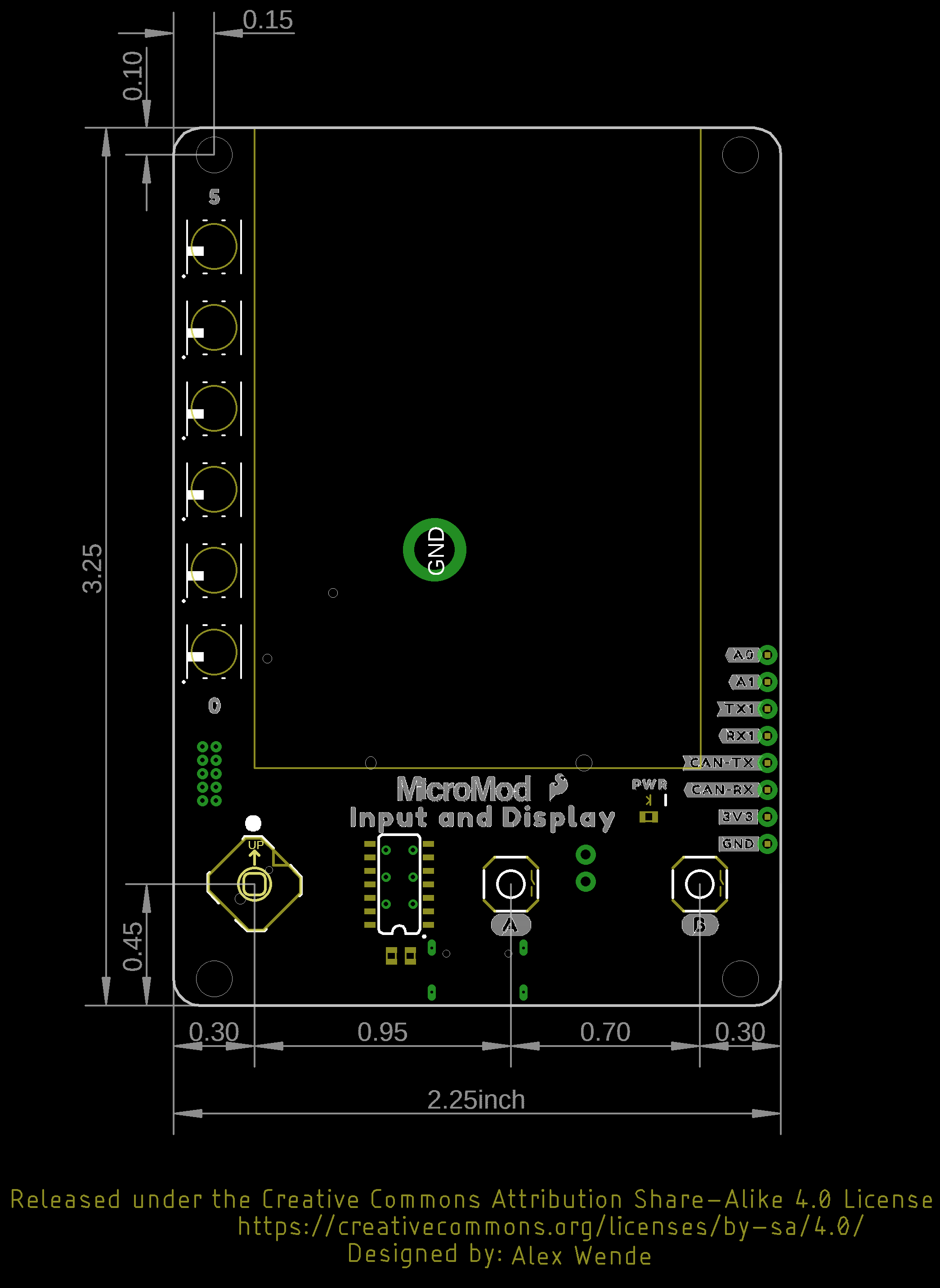
Board Dimensions
The Input and Display Carrier Board measures 3.25 inches by 2.25 inches.