MicroMod RP2040 Processor Board Hookup Guide
 bboyho
Hardware Overview
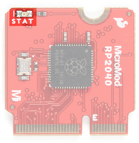
M.2 Connector
All of our MicroMod Processor Boards come equipped with the M.2 MicroMod Connector, which leverages the M.2 standard and specification to allow you to install your MicroMod Processor Board on your choice of carrier board. Most of the pins use a common pinout to ensure cross platform compatibility.
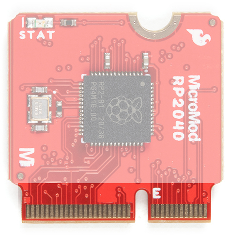
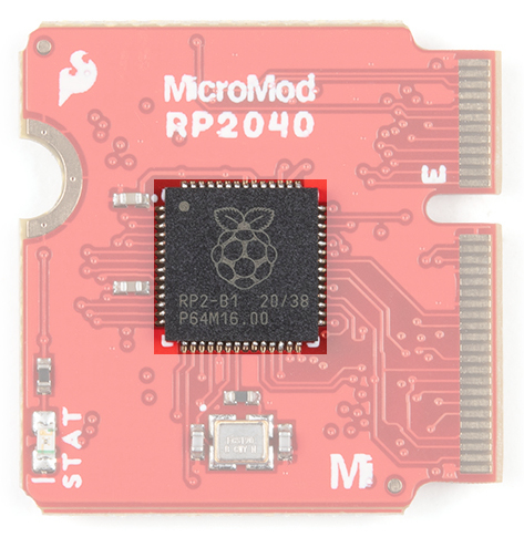
RP2040 Processor
The brains of the processor board is the Raspberry Pi Foundation's RP2040 ARM Cortex M0+ processor. An external 12MHz crystal is used as the clock for the RP2040. The RP2040 should be powered with 3.3V from a carrier board's M.2 connector. The logic levels for the I/O pins are 3.3V.
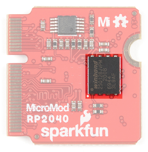
Flash Memory
On the back of the board is the W25Q128JVPIM, which adds 128Mb (16MB) of flash memory externally.
LED
A STAT LED is added to the top side of the board. This is useful debugging or as a status indicator. This is connected to GPIO25.
MicroMod RP2040 Processor Pin Functionality
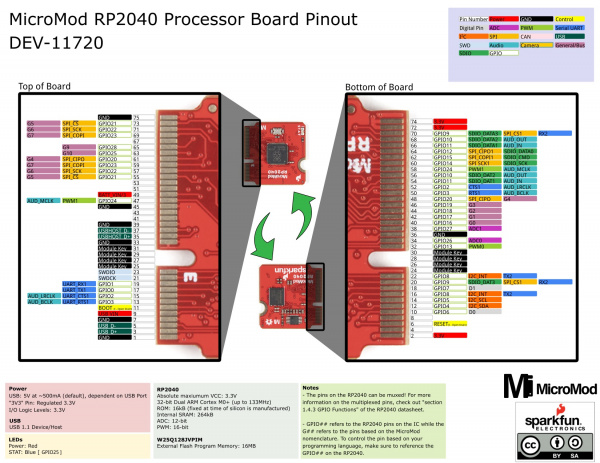
The complete pin map can be found in the table below or you can refer to the schematic.
Depending on your window size, you may need to use the horizontal scroll bar at the bottom of the table to view the additional pin functions. Note that the M.2 connector pins on opposing sides are offset from each other as indicated by the bottom pins where it says (Not Connected)*. There is no connection to pins that have a "-".
| AUDIO | UART | GPIO/BUS | I2C | SDIO | SPI | Dedicated |
| Alternate Function |
Primary Function |
RP2040 GPIO Pin | Bottom Pin |
Top Pin |
RP2040 GPIO Pin |
Primary Function |
Alternate Function |
||
|---|---|---|---|---|---|---|---|---|---|
| (Not Connected)* | 75 | GND | |||||||
| 3.3V | 74 | 73 | GPIO21 | ||||||
| 3.3V | 72 | 71 | GPIO22 | ||||||
| SPI_CS1 | SDIO_DATA3 | GPIO9 | 70 | 69 | GPIO23 | ||||
| AUD_OUT | SDIO_DATA2 | GPIO10 | 68 | 67 | - | ||||
| AUD_IN | SDIO_DATA1 | GPIO11 | 66 | 65 | GPIO28 | G9 | |||
| SDIO_DATA0 | SPI_CIPO1 | GPIO12 | 64 | 63 | GPIO25 | G10 | |||
| SDIO_CMD | SPI_COPI1 | GPIO15 | 62 | 61 | GPIO20 | SPI_CIPO | G4 | ||
| SDIO_SCK | SPI_SCK1 | GPIO14 | 60 | 59 | GPIO23 | SPI_COPI | G7 | ||
| AUD_MCLK | PWM1 | GPIO24 | 58 | 57 | GPIO22 | SPI_SCK | G6 | ||
| AUD_OUT | SDIO_DAT2 | GPIO10 | 56 | 55 | GPIO21 | SPI_CS | G5 | ||
| AUD_IN | SDIO_DAT1 | GPIO11 | 54 | 53 | - | ||||
| AUD_LRCLK | CTS1 | GPIO2 | 52 | 51 | - | ||||
| AUD_BCLK | UART_RTS1 | GPIO3 | 50 | 49 | BATT_VIN | ||||
| G4 | SPI_CIPO | GPIO20 | 48 | 47 | GPIO24 | PWM1 | AUD_MCLK | ||
| G3 | GPIO19 | 46 | 45 | GND | |||||
| G2 | GPIO18 | 44 | 43 | - | |||||
| G1 | GPIO17 | 42 | 41 | - | |||||
| G0 | GPIO16 | 40 | 39 | GND | |||||
| A1 | GPIO27 | 38 | 37 | USBHOST_D- | |||||
| GND | 36 | 35 | USBHOST_D+ | ||||||
| A0 | GPIO26 | 34 | 33 | GND | |||||
| PWM0 | GPIO13 | 32 | 31 | Module Key | |||||
| Module Key | 30 | 29 | Module Key | ||||||
| Module Key | 28 | 27 | Module Key | ||||||
| Module Key | 26 | 25 | Module Key | ||||||
| Module Key | 24 | 23 | SWDIO | ||||||
| I2C_INT | UART_TX2 | GPIO8 | 22 | 21 | SWDCK | ||||
| SPI_CS1 | SDIO_DAT3 | UART_RX2 | GPIO9 | 20 | 19 | GPIO1 | UART_RX1 | ||
| D1 | GPIO7 | 18 | 17 | GPIO0 | UART_TX1 | ||||
| TX2 | I2C_INT | GPIO8 | 16 | 15 | GPIO2 | UART_CTS1 | AUD_LRCLK | ||
| I2C_SCL | GPIO5 | 14 | 13 | GPIO3 | UART_RTS1 | AUD_BCLK | |||
| I2C_SDA | GPIO4 | 12 | 11 | BOOT | |||||
| D0 | GPIO6 | 10 | 9 | USB_VIN | |||||
| - | 8 | 7 | GND | ||||||
| RESET | 6 | 5 | USB_D- | ||||||
| - | 4 | 3 | USB_D+ | ||||||
| 3.3V_IN | 2 | 1 | GND | ||||||
| Function | Bottom Pin |
Top Pin |
Function | ||||||
|---|---|---|---|---|---|---|---|---|---|
| (Not Connected)* | 75 | GND | |||||||
| 3.3V | 74 | 73 | G5 / BUS5 | ||||||
| RTC_3V_BATT | 72 | 71 | G6 / BUS6 | ||||||
| SPI_CS1 | SDIO_DATA3 | 70 | 69 | G7 / BUS7 | |||||
| SDIO_DATA2 | 68 | 67 | G8 | ||||||
| SDIO_DATA1 | 66 | 65 | G9 | ADC_D- | CAM_HSYNC | ||||
| SPI_CIPO1 | SDIO_DATA0 | 64 | 63 | G10 | ADC_D+ | CAM_VSYNC | |||
| SPI COPI1 | SDIO_CMD | 62 | 61 | SPI_CIPO | |||||
| SPI SCK1 | SDIO_SCK | 60 | 59 | SPI_COPI | LED_DAT | ||||
| AUD_MCLK | 58 | 57 | SPI_SCK | LED_CLK | |||||
| CAM_MCLK | PCM_OUT | I2S_OUT | AUD_OUT | 56 | 55 | SPI_CS | |||
| CAM_PCLK | PCM_IN | I2S_IN | AUD_IN | 54 | 53 | I2C_SCL1 | |||
| PDM_DATA | PCM_SYNC | I2S_WS | AUD_LRCLK | 52 | 51 | I2C_SDA1 | |||
| PDM_CLK | PCM_CLK | I2S_SCK | AUD_BCLK | 50 | 49 | BATT_VIN / 3 (I - ADC) (0 to 3.3V) | |||
| G4 / BUS4 | 48 | 47 | PWM1 | ||||||
| G3 / BUS3 | 46 | 45 | GND | ||||||
| G2 / BUS2 | 44 | 43 | CAN_TX | ||||||
| G1 / BUS1 | 42 | 41 | CAN_RX | ||||||
| G0 / BUS0 | 40 | 39 | GND | ||||||
| A1 | 38 | 37 | USBHOST_D- | ||||||
| GND | 36 | 35 | USBHOST_D+ | ||||||
| A0 | 34 | 33 | GND | ||||||
| PWM0 | 32 | 31 | Module Key | ||||||
| Module Key | 30 | 29 | Module Key | ||||||
| Module Key | 28 | 27 | Module Key | ||||||
| Module Key | 26 | 25 | Module Key | ||||||
| Module Key | 24 | 23 | SWDIO | ||||||
| UART_TX2 | 22 | 21 | SWDCK | ||||||
| UART_RX2 | 20 | 19 | UART_RX1 | ||||||
| CAM_TRIG | D1 | 18 | 17 | UART_TX1 | |||||
| I2C_INT | 16 | 15 | UART_CTS1 | ||||||
| I2C_SCL | 14 | 13 | UART_RTS1 | ||||||
| I2C_SDA | 12 | 11 | BOOT (Open Drain) | ||||||
| D0 | 10 | 9 | USB_VIN | ||||||
| SWO | G11 | 8 | 7 | GND | |||||
| RESET# (Open Drain) | 6 | 5 | USB_D- | ||||||
| 3.3V_EN | 4 | 3 | USB_D+ | ||||||
| 3.3V | 2 | 1 | GND | ||||||
| Signal Group | Signal | I/O | Description | Voltage | Power | 3.3V | I | 3.3V Source | 3.3V |
|---|---|---|---|---|
| GND | Return current path | 0V | ||
| USB_VIN | I | USB VIN compliant to USB 2.0 specification. Connect to pins on processor board that require 5V for USB functionality | 4.8-5.2V | |
| RTC_3V_BATT | I | 3V provided by external coin cell or mini battery. Max draw=100μA. Connect to pins maintaining an RTC during power loss. Can be left NC. | 3V | |
| 3.3V_EN | O | Controls the carrier board's main voltage regulator. Voltage above 1V will enable 3.3V power path. | 3.3V | |
| BATT_VIN/3 | I | Carrier board raw voltage over 3. 1/3 resistor divider is implemented on carrier board. Amplify the analog signal as needed for full 0-3.3V range | 3.3V | |
| Reset | Reset | I | Input to processor. Open drain with pullup on processor board. Pulling low resets processor. | 3.3V |
| Boot | I | Input to processor. Open drain with pullup on processor board. Pulling low puts processor into special boot mode. Can be left NC. | 3.3V | |
| USB | USB_D± | I/O | USB Data ±. Differential serial data interface compliant to USB 2.0 specification. If UART is required for programming, USB± must be routed to a USB-to-serial conversion IC on the processor board. | |
| USB Host | USBHOST_D± | I/O | For processors that support USB Host Mode. USB Data±. Differential serial data interface compliant to USB 2.0 specification. Can be left NC. | |
| CAN | CAN_RX | I | CAN Bus receive data. | 3.3V |
| CAN_TX | O | CAN Bus transmit data. | 3.3V | |
| UART | UART_RX1 | I | UART receive data. | 3.3V |
| UART_TX1 | O | UART transmit data. | 3.3V | |
| UART_RTS1 | O | UART ready to send. | 3.3V | |
| UART_CTS1 | I | UART clear to send. | 3.3V | |
| UART_RX2 | I | 2nd UART receive data. | 3.3V | |
| UART_TX2 | O | 2nd UART transmit data. | 3.3V | |
| I2C | I2C_SCL | I/O | I2C clock. Open drain with pullup on carrier board. | 3.3V |
| I2C_SDA | I/O | I2C data. Open drain with pullup on carrier board | 3.3V | |
| I2C_INT# | I | Interrupt notification from carrier board to processor. Open drain with pullup on carrier board. Active LOW | 3.3V | |
| I2C_SCL1 | I/O | 2nd I2C clock. Open drain with pullup on carrier board. | 3.3V | |
| I2C_SDA1 | I/O | 2nd I2C data. Open drain with pullup on carrier board. | 3.3V | |
| SPI | SPI_COPI | O | SPI Controller Output/Peripheral Input. | 3.3V |
| SPI_CIPO | I | SPI Controller Input/Peripheral Output. | 3.3V | |
| SPI_SCK | O | SPI Clock. | 3.3V | |
| SPI_CS# | O | SPI Chip Select. Active LOW. Can be routed to GPIO if hardware CS is unused. | 3.3V | |
| SPI/SDIO | SPI_SCK1/SDIO_CLK | O | 2nd SPI Clock. Secondary use is SDIO Clock. | 3.3V |
| SPI_COPI1/SDIO_CMD | I/O | 2nd SPI Controller Output/Peripheral Input. Secondary use is SDIO command interface. | 3.3V | |
| SPI_CIPO1/SDIO_DATA0 | I/O | 2nd SPI Peripheral Input/Controller Output. Secondary use is SDIO data exchange bit 0. | 3.3V | |
| SDIO_DATA1 | I/O | SDIO data exchange bit 1. | 3.3V | |
| SDIO_DATA2 | I/O | SDIO data exchange bit 2. | 3.3V | |
| SPI_CS1/SDIO_DATA3 | I/O | 2nd SPI Chip Select. Secondary use is SDIO data exchange bit 3. | 3.3V | |
| Audio | AUD_MCLK | O | Audio master clock. | 3.3V |
| AUD_OUT/PCM_OUT/I2S_OUT/CAM_MCLK | O | Audio data output. PCM synchronous data output. I2S serial data out. Camera master clock. | 3.3V | |
| AUD_IN/PCM_IN/I2S_IN/CAM_PCLK | I | Audio data input. PCM syncrhonous data input. I2S serial data in. Camera periphperal clock. | 3.3V | |
| AUD_LRCLK/PCM_SYNC/I2S_WS/PDM_DATA | I/O | Audio left/right clock. PCM syncrhonous data SYNC. I2S word select. PDM data. | 3.3V | |
| AUD_BCLK/PCM_CLK/I2S_CLK/PDM_CLK | O | Audio bit clock. PCM clock. I2S continuous serial clock. PDM clock. | 3.3V | |
| SWD | SWDIO | I/O | Serial Wire Debug I/O. Connect if processor board supports SWD. Can be left NC. | 3.3V |
| SWDCK | I | Serial Wire Debug clock. Connect if processor board supports SWD. Can be left NC. | 3.3V | |
| ADC | A0 | I | Analog to digital converter 0. Amplify the analog signal as needed to enable full 0-3.3V range. | 3.3V |
| A1 | I | Analog to digital converter 1. Amplify the analog signal as needed to enable full 0-3.3V range. | 3.3V | |
| PWM | PWM0 | O | Pulse width modulated output 0. | 3.3V |
| PWM1 | O | Pulse width modulated output 1. | 3.3V | |
| Digital | D0 | I/O | General digital input/output pin. | 3.3V |
| D1/CAM_TRIG | I/O | General digital input/output pin. Camera trigger. | 3.3V | |
| General/Bus | G0/BUS0 | I/O | General purpose pins. Any unused processor pins should be assigned to Gx with ADC + PWM capable pins given priority (0, 1, 2, etc.) positions. The intent is to guarantee PWM, ADC and Digital Pin functionality on respective ADC/PWM/Digital pins. Gx pins do not guarantee ADC/PWM function. Alternative use is pins can support a fast read/write 8-bit or 4-bit wide bus. | 3.3V |
| G1/BUS1 | I/O | 3.3V | ||
| G2/BUS2 | I/O | 3.3V | ||
| G3/BUS3 | I/O | 3.3V | ||
| G4/BUS4 | I/O | 3.3V | ||
| G5/BUS5 | I/O | 3.3V | ||
| G6/BUS6 | I/O | 3.3V | ||
| G7/BUS7 | I/O | 3.3V | ||
| G8 | I/O | General purpose pin | 3.3V | |
| G9/ADC_D-/CAM_HSYNC | I/O | Differential ADC input if available. Camera horizontal sync. | 3.3V | |
| G10/ADC_D+/CAM_VSYNC | I/O | Differential ADC input if available. Camera vertical sync. | 3.3V | |
| G11/SWO | I/O | General purpose pin. Serial Wire Output | 3.3V |
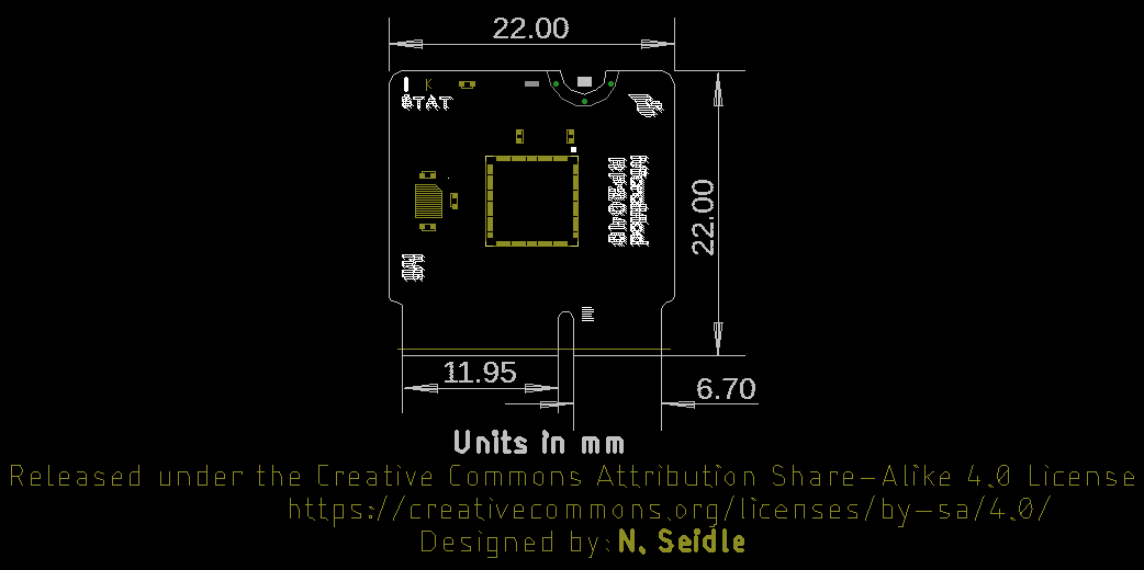
Board Dimensions
The board takes advantage of the standard MicroMod form factor.