MicroMod Ethernet Function Board - W5500 Hookup Guide
 El Duderino
Hardware Overview
Let's take a closer look at the hardware on the Ethernet Function Board - W5500 and how it interacts with the rest of the MicroMod ecosystem.
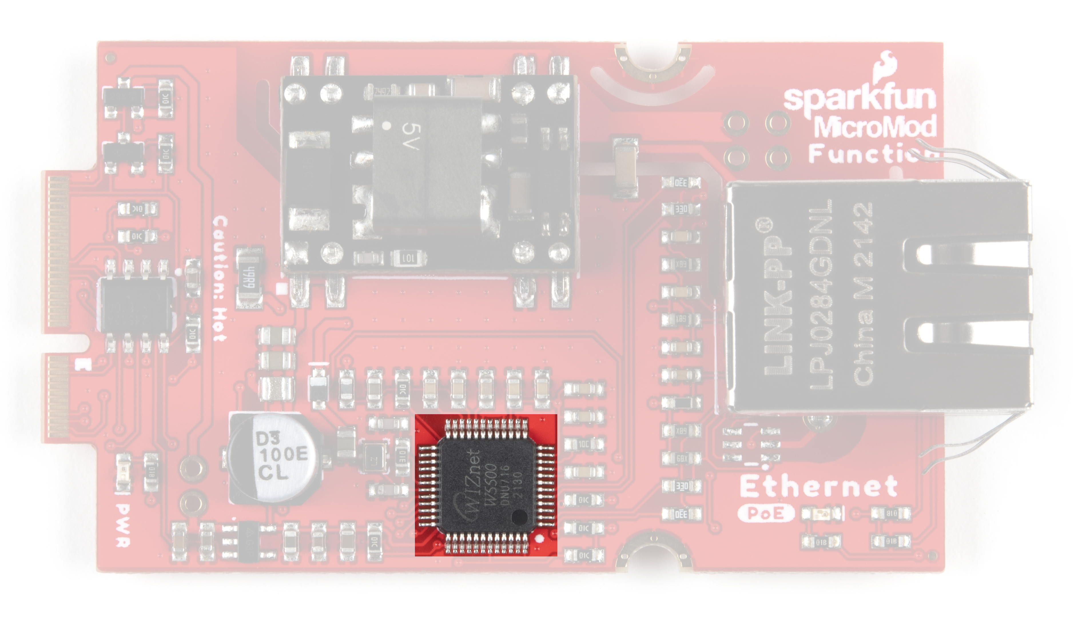
WIZnet W5500 Ethernet Controller
The W5500 Ethernet Controller from WIZnet is a TCP/IP embedded Ethernet controller that uses SPI communication protocol to allow up to eight independent sockets operate simultaneously.
- TCP
- UDP
- ICMP
- IPv4
- ARP
- IGMP
- PPPoE
The W5500 SPI interface operates at up to 80MHz and supports fast SPI for high speed Ethernet communication. The chip also includes a Wake on Lan (WOL) operation and power down mode to help conserve power. The W5500 operates at 3.3V but has 5V-tolerant I/O. For detailed information on the W5500, refer to the datasheet.
The Function Board includes three solder jumpers connected to the three network mode selection pins to allow users to configure the W5500 network operation mode. By default, the board sets the W5500 to operates in 10/100Base-T with Auto-Negotiation enabled. Read on to the Solder Jumpers portion of this section or refer to the pin descriptions in the datasheet for more information on adjusting the operation mode.
Power
The Ethernet Function Board - W5500 features several power input options including PoE and USB (via the Main Board). By default, the board acts as a PoE Powered Device (PD), receiving voltage over the Ethernet connection using the IEEE802.3af Alternative B power scheme.
The Alternate B power scheme uses the spare pairs (pins 4/5 and 7/8) in the Ethernet cable for positive and negative DC voltage, keeping things simple if any troubleshooting is needed. The board includes a pair of PoE isolation jumpers that allows users to isolate these pins from the DC/DC converter input. When opened, the MicroMod assembly can receive power over USB, LiPo battery or through the DC/DC converter input PTH pins. The USB and LiPo power inputs are isolated from the PoE circuit.
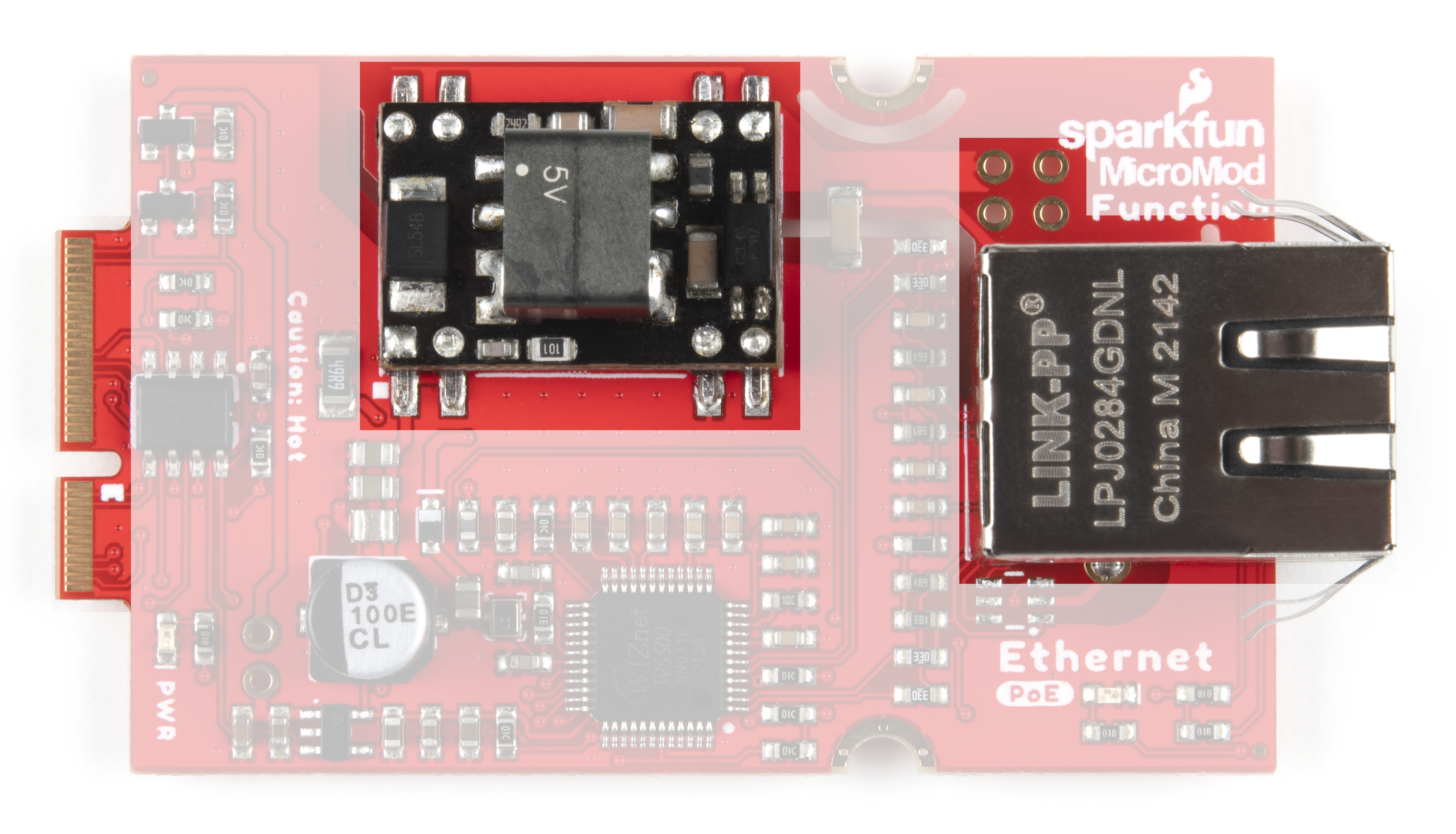
DC/DC Converter Circuit
The board uses an Ag9905M Power-over-Ethernet (PoE) DC/DC converter to provide 5V from an Ethernet connection. For complete information on the Ag9905M, refer to the datasheet.
The Ag9905 accepts an input voltage between 36V and 57V but a voltage of 48V or greater is recommended on initial powerup to ensure the module functions properly. After power up, input voltage can be reduced to 36V if needed.
The Ag9905 provides 9 Watts of power for the MicroMod system and any peripheral devices connected to it (i.e. Qwiic breakouts, etc.). The 5V output from the converter is filtered to reduce noise for 5V circuits on the board and is also regulated down to 3.3V.
RJ45 Connector
The RJ45 connector on this function board includes embedded magnetics for PoE applications and is MagJack®-Compatible.
The Function Board uses all pairs on the RJ45 connector by default as the PoE configuration uses the spare pair for power inputs. Users who do not wish to use PoE can isolate these pins for other use by opening the PoE Isolation Jumpers. Reminder, if the PoE pairs are disconnected, power must be supplied from another source, either USB, LiPo battery or via the DC/DC converter input PTH pins on the other side of the PoE Isolation Jumpers.
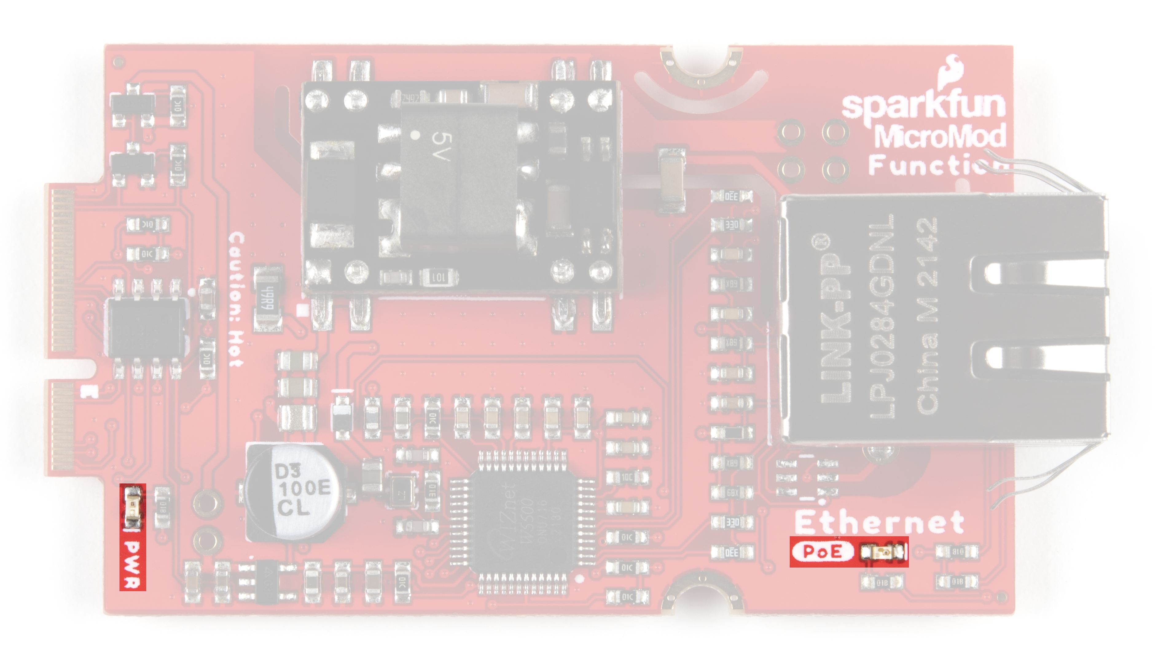
LEDs
The board has a pair of status LEDs indicating general power and PoE power as well as the pair of LEDs on the RJ45 connector for Link and Activity statuses.
Solder Jumpers
There are thirteen solder jumpers on the Function Board. The table below outlines their labels and functions:
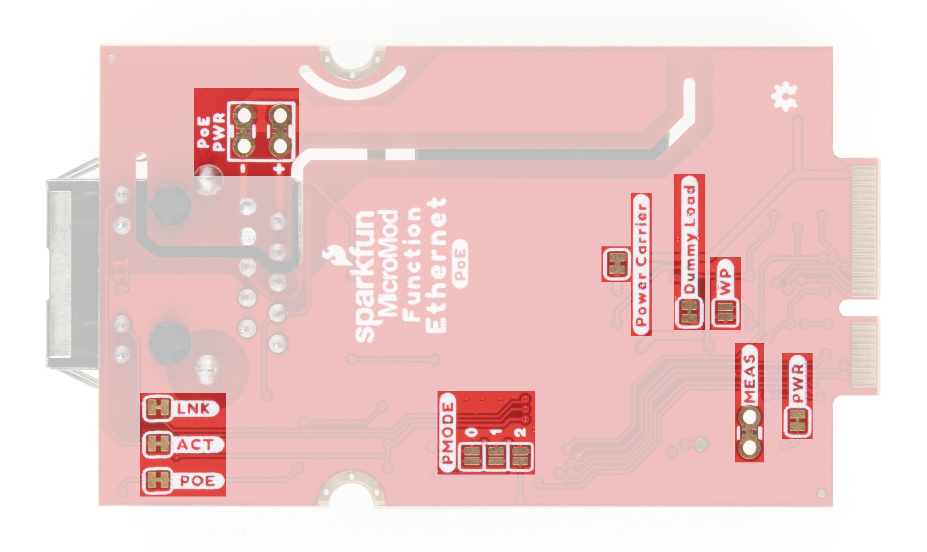
| Label | Default State | Function | Notes |
|---|---|---|---|
| PWR | CLOSED | Completes Power LED circuit. | Open to disable Power LED. |
| MEAS | CLOSED | Completes VCC circuit tying VCC to 5V input. | Open to measure current drawn by the Function Board. |
| WP | OPEN | Pulls EEPROM Write Protect pin to 3.3V/HIGH | Close to pull this pin to 0V/LOW to disable write protect. |
| Dummy Load | CLOSED | Creates a dummy load of 100mA on the DC/DC converter output. | Open to disable the dummy load. |
| Power Carrier | CLOSED | Selects power configuration (PoE or USB). | Open to disable PoE for VCC_In. |
| LNK | CLOSED | Completes the RJ45 Link LED circuit. | Open to disable the Link LED. |
| ACT | CLOSED | Completes the RJ45 Activity LED circuit. | Open to disable the Activity LED. |
| POE | CLOSED | Completes the PoE Status LED circuit. | Open to disable the PoE Status LED. |
| POE Power (Pair) | CLOSED | Ties the PoE +/- pins to DC/DC converter input. | Open both to isolate Ethernet pairs used for PoE from the DC/DC converter input. |
| PMODE0 | OPEN | Ties PMODE0 to 3.3V/HIGH. | Adjust this in tandem with the other two PMODE jumpers to switch network modes on the W5500.1 |
| PMODE1 | OPEN | Ties PMODE1 to 3.3V/HIGH. | Adjust this in tandem with the other two PMODE jumpers to switch network modes on the W5500.1 |
| PMODE2 | OPEN | Ties PMODE2 to 3.3V/HIGH. | Adjust this in tandem with the other two PMODE jumpers to switch network modes on the W5500.1 |
MicroMod Function Board Pinout
This Function Board uses the following pins on a connected Processor Board:
- 3.3V & VCC
- Power Enable
- SPI - W5500 Communication
- I2C - EEPROM Communication
- D0 (Slot 0) / D1 (Slot 1) - W5500 Interrupt
- CS0 (Slot 0) / CS1 (Slot 1) - W5500 Chip Select (SPI)
- PWM0 (Slot 0) - PWM1 (Slot 1) W5500 Reset
For the complete MicroMod Pinout and pins used by this function board, take a look at the tables below:
| AUDIO | UART | GPIO/BUS | I2C | SDIO | SPI0 | Dedicated |
| Function | Bottom Pin |
Top Pin |
Function | ||||||
|---|---|---|---|---|---|---|---|---|---|
| (Not Connected) | 75 | GND | |||||||
| 3.3V | 74 | 73 | G5 / BUS5 | ||||||
| RTC_3V_BATT | 72 | 71 | G6 / BUS6 | ||||||
| SPI_CS1# | SDIO_DATA3 (I/O) | 70 | 69 | G7 / BUS7 | |||||
| SDIO_DATA2 (I/O) | 68 | 67 | G8 | ||||||
| SDIO_DATA1 (I/O) | 66 | 65 | G9 | ADC_D- | CAM_HSYNC | ||||
| SPI_CIPO1 | SDIO_DATA0 (I/O) | 64 | 63 | G10 | ADC_D+ | CAM_VSYNC | |||
| SPI COPI1 | SDIO_CMD (I/O) | 62 | 61 | SPI_CIPO (I) | |||||
| SPI SCK1 | SDIO_SCK (O) | 60 | 59 | SPI_COPI (O) | LED_DAT | ||||
| AUD_MCLK (O) | 58 | 57 | SPI_SCK (O) | LED_CLK | |||||
| CAM_MCLK | PCM_OUT | I2S_OUT | AUD_OUT | 56 | 55 | SPI_CS# | |||
| CAM_PCLK | PCM_IN | I2S_IN | AUD_IN | 54 | 53 | I2C_SCL1 (I/O) | |||
| PDM_DATA | PCM_SYNC | I2S_WS | AUD_LRCLK | 52 | 51 | I2C_SDA1 (I/O) | |||
| PDM_CLK | PCM_CLK | I2S_SCK | AUD_BCLK | 50 | 49 | BATT_VIN / 3 (I - ADC) (0 to 3.3V) | |||
| G4 / BUS4 | 48 | 47 | PWM1 | ||||||
| G3 / BUS3 | 46 | 45 | GND | ||||||
| G2 / BUS2 | 44 | 43 | CAN_TX | ||||||
| G1 / BUS1 | 42 | 41 | CAN_RX | ||||||
| G0 / BUS0 | 40 | 39 | GND | ||||||
| A1 | 38 | 37 | USBHOST_D- | ||||||
| GND | 36 | 35 | USBHOST_D+ | ||||||
| A0 | 34 | 33 | GND | ||||||
| PWM0 | 32 | 31 | Module Key | ||||||
| Module Key | 30 | 29 | Module Key | ||||||
| Module Key | 28 | 27 | Module Key | ||||||
| Module Key | 26 | 25 | Module Key | ||||||
| Module Key | 24 | 23 | SWDIO | ||||||
| UART_TX2 (O) | 22 | 21 | SWDCK | ||||||
| UART_RX2 (I) | 20 | 19 | UART_RX1 (I) | ||||||
| CAM_TRIG | D1 | 18 | 17 | UART_TX1 (0) | |||||
| I2C_INT# | 16 | 15 | UART_CTS1 (I) | ||||||
| I2C_SCL (I/0) | 14 | 13 | UART_RTS1 (O) | ||||||
| I2C_SDA (I/0) | 12 | 11 | BOOT (I - Open Drain) | ||||||
| D0 | 10 | 9 | USB_VIN | ||||||
| SWO | G11 | 8 | 7 | GND | |||||
| RESET# (I - Open Drain) | 6 | 5 | USB_D- | ||||||
| 3.3V_EN | 4 | 3 | USB_D+ | ||||||
| 3.3V | 2 | 1 | GND | ||||||
| Description | Function | Bottom Pin |
Top Pin |
Function | Description |
|---|---|---|---|---|---|
| (Not Connected) | 75 | GND | |||
| - | 74 | 73 | 3.3V | Power Supply: 3.3-6V | |
| - | 72 | 71 | Power EN | Power Enable | |
| - | 70 | 69 | - | ||
| - | 66 | 65 | - | ||
| - | 64 | 63 | - | ||
| - | 62 | 61 | - | ||
| - | 60 | 59 | - | ||
| - | 58 | 57 | - | ||
| - | 56 | 55 | - | . | |
| - | 54 | 53 | - | ||
| - | 52 | 51 | ETH_RST | W5500 Reset. | |
| - | 50 | 49 | ETH_CS | W5500 Chip Select | |
| - | 48 | 47 | ETH_INT | W550 Interrupt Pin | |
| - | 46 | 45 | GND | ||
| - | 44 | 43 | - | ||
| - | 42 | 41 | - | ||
| Write protection pin for the EEPROM. Pull low to enable. | EEPROM_WP | 40 | 39 | GND | |
| - | 38 | 37 | - | ||
| EEPROM I2C address configuration. | EEPROM_A0 | 36 | 35 | - | |
| EEPROM I2C address configuration. | EEPROM_A1 | 34 | 33 | GND | |
| EEPROM I2C address configuration. | EEPROM_A2 | 32 | 31 | Module Key | |
| Module Key | 30 | 29 | Module Key | ||
| Module Key | 28 | 27 | Module Key | ||
| Module Key | 26 | 25 | Module Key | ||
| Module Key | 24 | 23 | - | ||
| - | 22 | 21 | I2C_SCL | I2C - Clock signal for EEPROM | |
| - | 20 | 19 | I2C_SDA | I2C - Data signal for EEPROM | |
| - | 18 | 17 | - | ||
| - | 16 | 15 | - | ||
| - | 14 | 13 | - | ||
| - | 12 | 11 | - | ||
| - | 10 | 9 | - | ||
| - | 8 | 7 | POCI | SPI Peripheral Output/Controller Input. | |
| - | 6 | 5 | PICO | SPI Peripheral Input/Controller Output. | |
| - | 4 | 3 | SCK | SPI Clock Signal | |
| - | 2 | 1 | GND |
| Signal Group | Signal | I/O | Description | Voltage | Power | 3.3V | I | 3.3V Source | 3.3V |
|---|---|---|---|---|
| GND | Return current path | 0V | ||
| USB_VIN | I | USB VIN compliant to USB 2.0 specification. Connect to pins on processor board that require 5V for USB functionality | 4.8-5.2V | |
| RTC_3V_BATT | I | 3V provided by external coin cell or mini battery. Max draw=100μA. Connect to pins maintaining an RTC during power loss. Can be left NC. | 3V | |
| 3.3V_EN | O | Controls the carrier board's main voltage regulator. Voltage above 1V will enable 3.3V power path. | 3.3V | |
| BATT_VIN/3 | I | Carrier board raw voltage over 3. 1/3 resistor divider is implemented on carrier board. Amplify the analog signal as needed for full 0-3.3V range | 3.3V | |
| Reset | Reset | I | Input to processor. Open drain with pullup on processor board. Pulling low resets processor. | 3.3V |
| Boot | I | Input to processor. Open drain with pullup on processor board. Pulling low puts processor into special boot mode. Can be left NC. | 3.3V | |
| USB | USB_D± | I/O | USB Data ±. Differential serial data interface compliant to USB 2.0 specification. If UART is required for programming, USB± must be routed to a USB-to-serial conversion IC on the processor board. | |
| USB Host | USBHOST_D± | I/O | For processors that support USB Host Mode. USB Data±. Differential serial data interface compliant to USB 2.0 specification. Can be left NC. | |
| CAN | CAN_RX | I | CAN Bus receive data. | 3.3V |
| CAN_TX | O | CAN Bus transmit data. | 3.3V | |
| UART | UART_RX1 | I | UART receive data. | 3.3V |
| UART_TX1 | O | UART transmit data. | 3.3V | |
| UART_RTS1 | O | UART ready to send. | 3.3V | |
| UART_CTS1 | I | UART clear to send. | 3.3V | |
| UART_RX2 | I | 2nd UART receive data. | 3.3V | |
| UART_TX2 | O | 2nd UART transmit data. | 3.3V | |
| I2C | I2C_SCL | I/O | I2C clock. Open drain with pullup on carrier board. | 3.3V |
| I2C_SDA | I/O | I2C data. Open drain with pullup on carrier board | 3.3V | |
| I2C_INT# | I | Interrupt notification from carrier board to processor. Open drain with pullup on carrier board. Active LOW | 3.3V | |
| I2C_SCL1 | I/O | 2nd I2C clock. Open drain with pullup on carrier board. | 3.3V | |
| I2C_SDA1 | I/O | 2nd I2C data. Open drain with pullup on carrier board. | 3.3V | |
| SPI | SPI_PICO | O | SPI Peripheral Input/Controller Output. | 3.3V |
| SPI_POCI | I | SPI Peripheral Output/Controller Input. | 3.3V | |
| SPI_SCK | O | SPI Clock. | 3.3V | |
| SPI_CS# | O | SPI Chip Select. Active LOW. Can be routed to GPIO if hardware CS is unused. | 3.3V | |
| SPI/SDIO | SPI_SCK1/SDIO_CLK | O | 2nd SPI Clock. Secondary use is SDIO Clock. | 3.3V |
| SPI_PICO1/SDIO_CMD | I/O | 2nd SPI Peripheral Input/Controller Output. Secondary use is SDIO command interface. | 3.3V | |
| SPI_POCI1/SDIO_DATA0 | I/O | 2nd SPI Controller Output/Peripheral Input. Secondary use is SDIO data exchange bit 0. | 3.3V | |
| SDIO_DATA1 | I/O | SDIO data exchange bit 1. | 3.3V | |
| SDIO_DATA2 | I/O | SDIO data exchange bit 2. | 3.3V | |
| SPI_CS1/SDIO_DATA3 | I/O | 2nd SPI Chip Select. Secondary use is SDIO data exchange bit 3. | 3.3V | |
| Audio | AUD_MCLK | O | Audio master clock. | 3.3V |
| AUD_OUT/PCM_OUT/I2S_OUT/CAM_MCLK | O | Audio data output. PCM synchronous data output. I2S serial data out. Camera master clock. | 3.3V | |
| AUD_IN/PCM_IN/I2S_IN/CAM_PCLK | I | Audio data input. PCM syncrhonous data input. I2S serial data in. Camera periphperal clock. | 3.3V | |
| AUD_LRCLK/PCM_SYNC/I2S_WS/PDM_DATA | I/O | Audio left/right clock. PCM syncrhonous data SYNC. I2S word select. PDM data. | 3.3V | |
| AUD_BCLK/PCM_CLK/I2S_CLK/PDM_CLK | O | Audio bit clock. PCM clock. I2S continuous serial clock. PDM clock. | 3.3V | |
| SWD | SWDIO | I/O | Serial Wire Debug I/O. Connect if processor board supports SWD. Can be left NC. | 3.3V |
| SWDCK | I | Serial Wire Debug clock. Connect if processor board supports SWD. Can be left NC. | 3.3V | |
| ADC | A0 | I | Analog to digital converter 0. Amplify the analog signal as needed to enable full 0-3.3V range. | 3.3V |
| A1 | I | Analog to digital converter 1. Amplify the analog signal as needed to enable full 0-3.3V range. | 3.3V | |
| PWM | PWM0 | O | Pulse width modulated output 0. | 3.3V |
| PWM1 | O | Pulse width modulated output 1. | 3.3V | |
| Digital | D0 | I/O | General digital input/output pin. | 3.3V |
| D1/CAM_TRIG | I/O | General digital input/output pin. Camera trigger. | 3.3V | |
| General/Bus | G0/BUS0 | I/O | General purpose pins. Any unused processor pins should be assigned to Gx with ADC + PWM capable pins given priority (0, 1, 2, etc.) positions. The intent is to guarantee PWM, ADC and Digital Pin functionality on respective ADC/PWM/Digital pins. Gx pins do not guarantee ADC/PWM function. Alternative use is pins can support a fast read/write 8-bit or 4-bit wide bus. | 3.3V |
| G1/BUS1 | I/O | 3.3V | ||
| G2/BUS2 | I/O | 3.3V | ||
| G3/BUS3 | I/O | 3.3V | ||
| G4/BUS4 | I/O | 3.3V | ||
| G5/BUS5 | I/O | 3.3V | ||
| G6/BUS6 | I/O | 3.3V | ||
| G7/BUS7 | I/O | 3.3V | ||
| G8 | I/O | General purpose pin | 3.3V | |
| G9/ADC_D-/CAM_HSYNC | I/O | Differential ADC input if available. Camera horizontal sync. | 3.3V | |
| G10/ADC_D+/CAM_VSYNC | I/O | Differential ADC input if available. Camera vertical sync. | 3.3V | |
| G11/SWO | I/O | General purpose pin. Serial Wire Output | 3.3V |
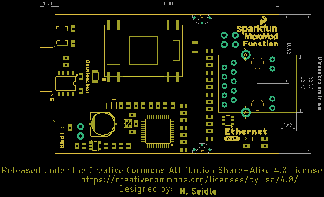
Board Dimensions
The MicroMod Ethernet Function Board matches the MicroMod Function Board standard and measures 1.50" x 2.56" (38.1mm x 65.024mm).