MicroMod Data Logging Carrier Board Hookup Guide
 El Duderino,
  Nate
Nate 
Hardware Overview
In this section we'll cover the components on the MicroMod Data Logging Carrier Board, how a specific MicroMod Processor Board interacts with it and highlight a few unique features on the board.
Common Components
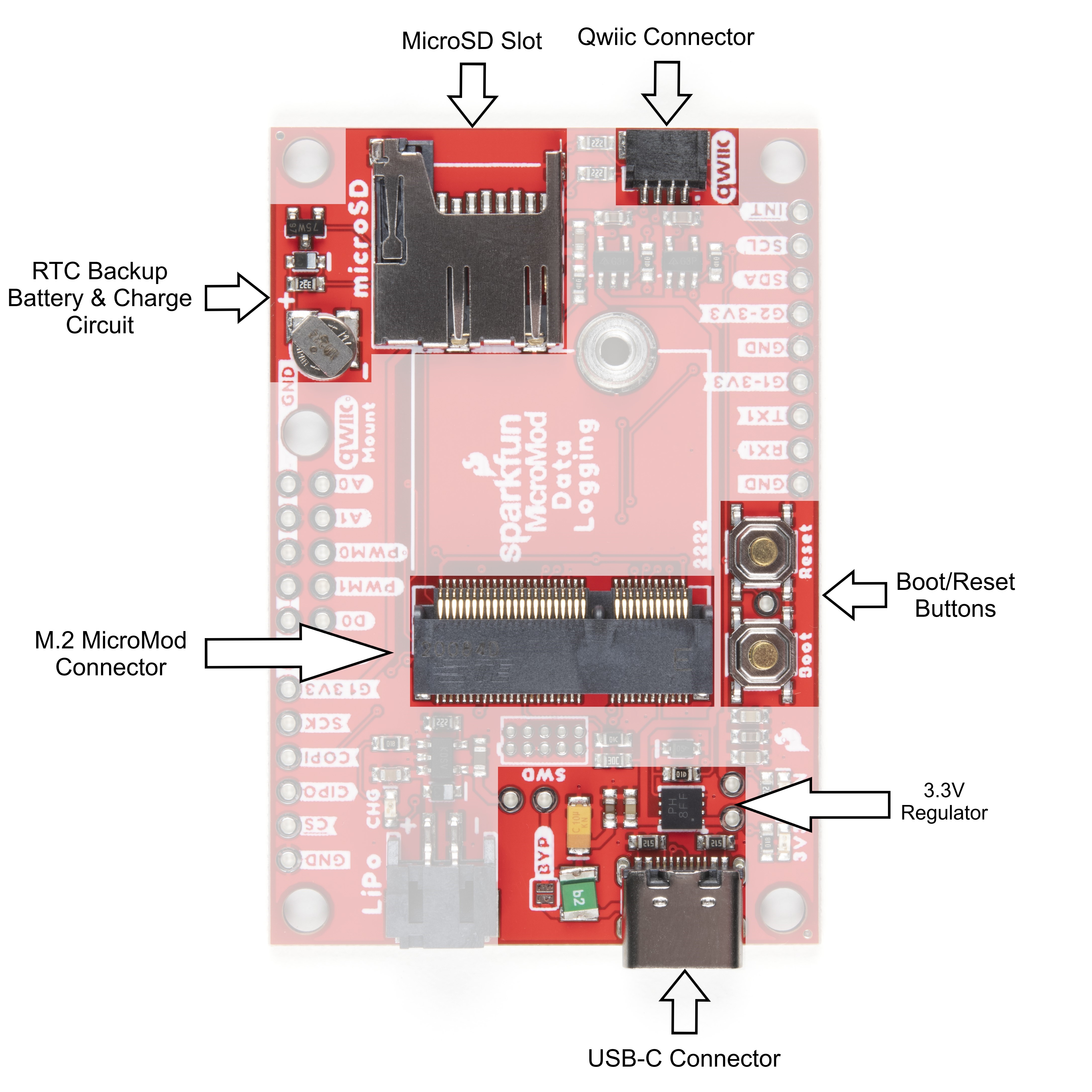
Most SparkFun MicroMod Carrier Boards will have some common components and all MicroMod Carrier Boards will have the keyed M.2 MicroMod Connector to plug your processor into. The photo and list below outline some of the components included on most SparkFun MicroMod Carrier Boards.
- M.2 MicroMod Connector - This special keyed M.2 connector lets you install your MicroMod Processor Board of choice on your Carrier Board.
- USB-C Connector - Connect to your computer to program your Processor Board and also can provide power to your MicroMod system.
- 3.3V Regulator - Provides a regulated 3.3V and sources up to 1A.
- Qwiic Connector - The standard Qwiic connector so you can add Qwiic devices to your MicroMod system.
- Boot/Reset Buttons - Push buttons to enter boot mode on Processor Boards and to reset your MicroMod circuit.
- RTC Backup Battery & Charge Circuit - 1mAh backup battery for the RTC for certain MicroMod Processor Boards . Receives charge voltage from 3.3V.
- microSD Slot - Insert a µSD card formatted to FAT32 here to log your data.
Power Control Circuit
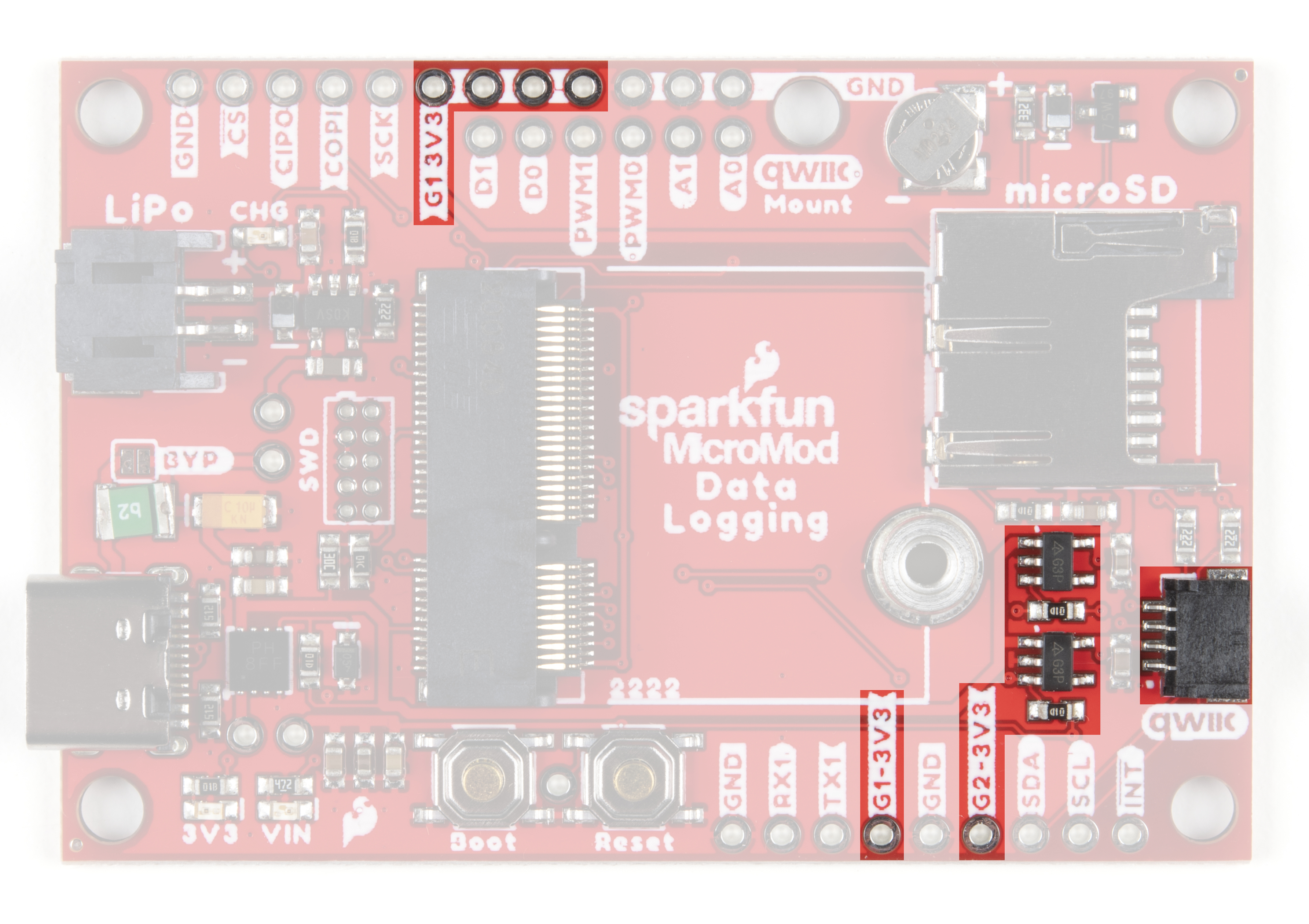
The Data Logging Carrier Board features two 3.3V/600mA voltage regulators that have their Enable pins tied to I/O pins on an attached MicroMod Processor Board. This allows control of the regulators' output with a few lines of code making it extremely simple to control and conserve power in battery-powered applications. The G1-3V3 line is controlled by G1 on the MicroMod Processor and the G2-3.3V circuit is (as you may suspect) is controlled by G2 on the MicroMod Processor. The G1-3.3V power circuit is tied to several pins highlighted in the below photo for extra flexibility powering external devices. The G2-3V3 output is tied to the 3.3V pin on the Qwiic connector as well as a dedicated PTH pin labeled G2-3V3.
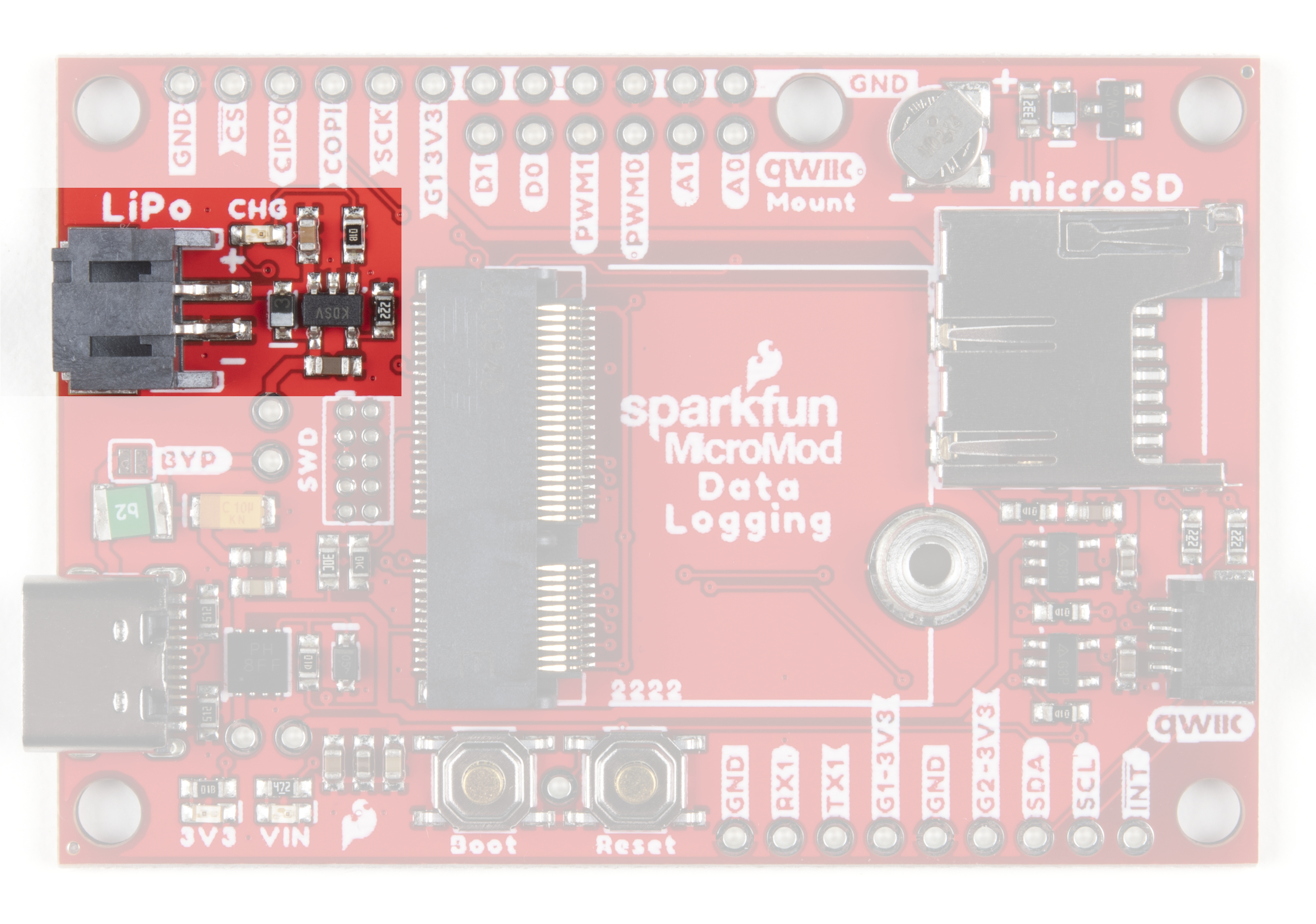
Battery Charging Circuit
The board also has a MCP73831 Single-Cell Lithium-Ion/Lithium-Polymer Charge IC so you can charge an attached single-cell LiPo battery. The charge IC receives power primarily from USB and can source up to 450mA to charge an attached battery.
Data Logging Connections
Along with the Qwiic connector mentioned in the Common Components, the Data Logging Carrier Board breaks out several other pins to connect UART, SPI and other I/O devices. The primary SPI pins are netted to the µSD slot and a PTH header near the LiPo battery connector. A second Chip Select pin tied to G0 is broken out to that same header.
A UART PTH header connects to RX1 and TX1 for serial data logging and A0, A1, PWM0, PWM1, D0 and D1 are routed to dedicated PTH pins as well. Lastly, if users prefer a soldered connection instead of Qwiic, the primary I2C bus is broken out to PTH pins.

JTAG
An unpopulated JTAG footprint is available for more advanced users who need breakpoint level debugging. We recommend checking out our JTAG section for the compatible male header and a compatible JTAG programmer and debugger.

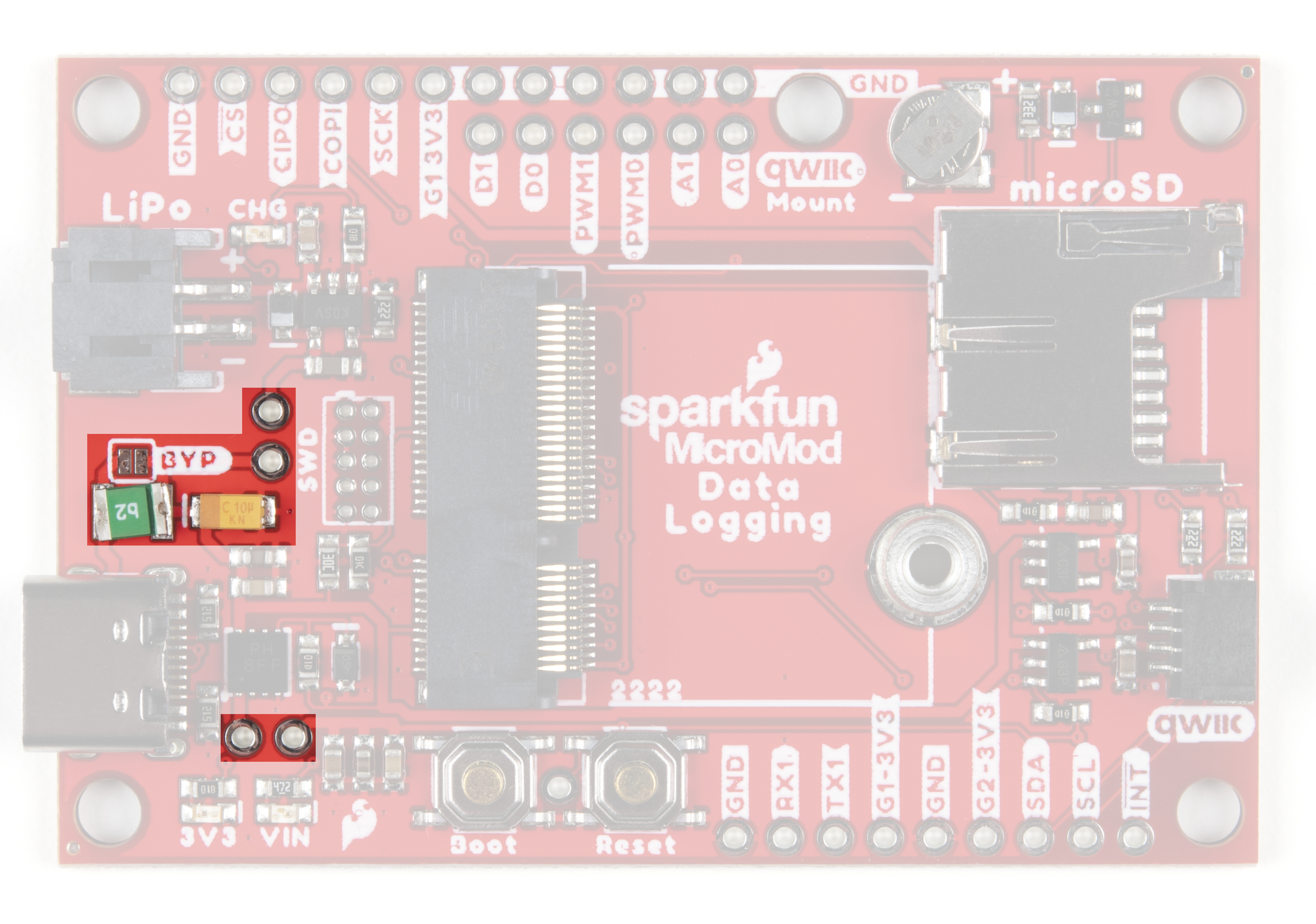
Solder Jumpers
There are seven solder jumpers on the Data Logging Carrier Board labeled I2C, MEAS, BYP, VIN, 3V3, VE, and BATT. In this section we'll detail the functionality and default states of each jumper.
| Jumper Name/Label | Description | Default State |
|---|---|---|
| I2C Pull-Up / I2C | Pulls the Qwiic SDA/SCL lines to 3.3V via two 2.2KΩ resistors | CLOSED |
| Measure / MEAS | Open this jumper to probe the current draw at the 3.3V output of the regulator. For help measuring current, take a look at our How to Use a Multimeter tutorial. | CLOSED |
| Bypass / BYP | The "penny-in-the-fuse" jumper. Bypasses the 6V/2A fuse and nets VIN and V_USB together to allow >2A current flows. Close only if you know what you are doing! | OPEN |
| VIN / VIN_LED | Connects the 5V/VIN LED to 3.7-6V (typ. 5V from USB) via a 4.1KΩ resistor. Open to disable the VIN LED. | CLOSED |
| 3V3 / 3V3_LED | Connects the 3.3V LED to 3.3V via a 1KΩ resistor. Open to disable the 3.3V LED. | CLOSED |
| Voltage Enable / VE | Close this jumper to enable processor control of the 3.3V bus. | OPEN |
| Battery / BATT | Open this jumper to measure current draw from the battery or to switch primary power from USB to battery. | CLOSED |
 |
 |
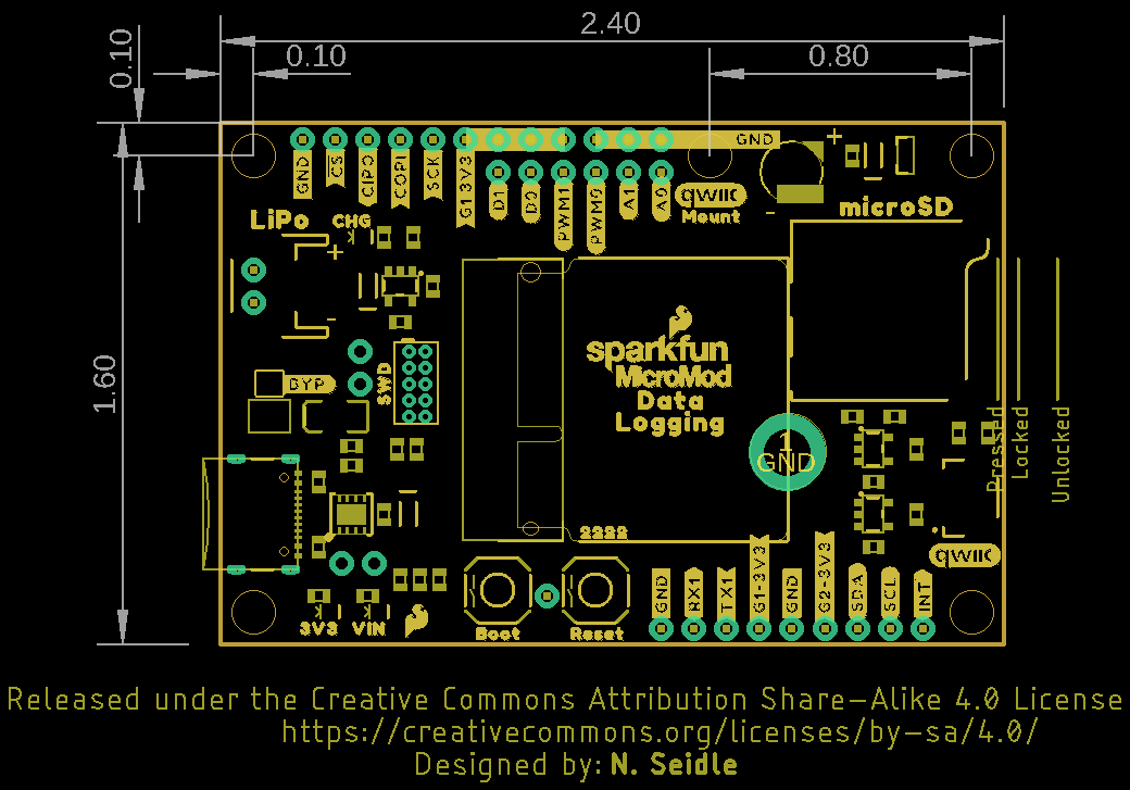
Board Dimensions
The MicroMod Data Logging Carrier Board measures 2.40" x 1.60" (60.96mm x 40.64mm) and has five mounting holes that fit a 4-40 screw. Take note of the mounting hole labeled "Qwiic Mount" above the µSD slot as it can work as single mount for a Qwiic breakout (or other sensor) or you can pair it with the outer mount in the "top-right" corner for a more secure mounting option. We demonstrate using these two mounts for a Qwiic breakout in the following section, Hardware Assembly.
Now that we're familiar with the hardware on the MicroMod Data Logging Carrier Board, it's time to plug your Processor Board and peripheral sensors in and start logging some data. Next up we'll cover some assembly tips.