Designing PCBs: SMD Footprints
 Nate
Nate 
Footprint Creation
Eagle requires three things to get an IC into the library:
- Package (also known as a footprint)
- Symbol (the schematic symbol)
- Device (mapping them together)
The tutorial images show us working from the SparkFun-DigitalIC.lbr file but you can create your own custom library file if you'd like.
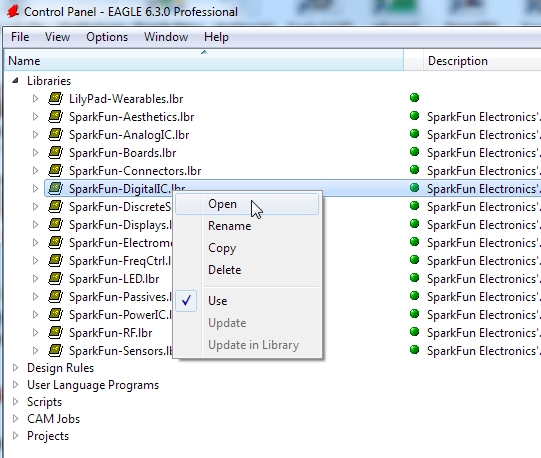
We are going to start by creating a footprint from scratch. Because the FT230X is a digital IC, let’s open the SparkFun-DigitalIC library.
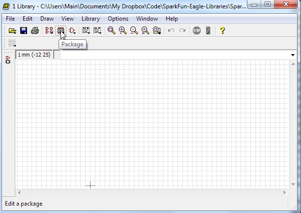
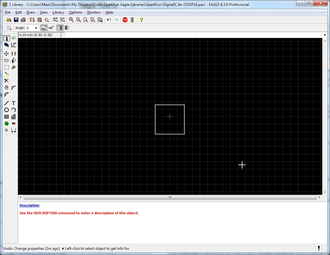
We’ve got a clean slate! Click on ‘package’

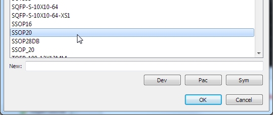
Now bring up the datasheet for the FT230X and skim down to where the package is described. This IC uses a package type called SSOP16 and has 16 pins. Wikipedia has some good information about SSOP (Shrink small-outline package) chips. For our purposes, we need only to get a short package identifier into Eagle.
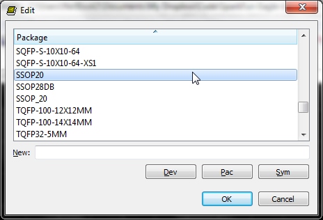
From within the Eagle footprint list, click on any footprint in this window and press ‘s’. This will bring you to the packages starting with the letter S. Now is your chance to see if the package you are about to create is already available. In our case, ‘SSOP20’ is available but SSOP16 (the 16 derivative) is not.
To create a new package, type the name SSOP16 into the 'New:' box. This fits with the same naming structure as the SSOP20 package.
Do you already have a SSOP16 in your library? (Look at you, you have the most up to date library!) Go ahead and call this one ‘SSOP16-PRACTICE’ or some such name that you can find later.
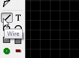
Now we’ve got a black window of nothing. From the datasheet, this IC is E1 (0.154”) wide and D (0.193”) long. For now, let’s create a square on the tDocu (top document) layer. Click on ‘Wire’.
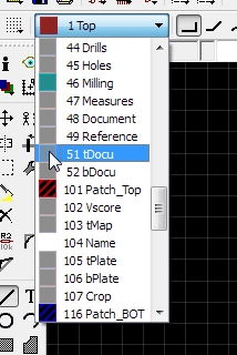
We can now draw, but we need to get to the tDocu layer. To do this you can either drop down the layers menu and select layer 51 tDocu or...
click the center button/scroll wheel on your mouse. I much prefer using the scroll wheel to select the layer because I jump to different layers a lot. You’ll see a ton of different layers. Find layer 51 and click it.
Draw a box. Hit escape to stop drawing. This is not really the shape of the IC. To get the exact shape, let’s look at the dimensions of the IC again. 0.154” wide and 0.193” long. Every manufacturer will have different tolerances. Use the nominal (NOM) dimension when it is provided. If you only have MIN and MAX dimensions, I will use the usually take the midpoint between them.
In Eagle, we want the component to have 0,0 centrally located within the component. So if the X dimension is 0.193 the left side of the box will be -0.0965, right side will be 0.0965. Let’s modify the left and right sides to be at these X locations.
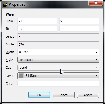
Click the ‘i’ button and then select the left gray bar by left clicking on it. We are now modifying the X and Y coordinates of the starting and ending points of this line. Note that in this picture by line is -3,2 to -3,-3. I’m on the wrong grid! I’m on the metric grid but our dimensions are in imperial. This is a common problem and you will be jumping between grid types often.
To switch between grid types, exit out of any window, then hit F10 for the standard imperial grid and Alt+F10 for the metric grid.
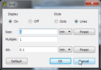
To change the grid to something really wild, click on the Grid button in the upper left corner of the menu bar. Here you can modify many different settings. In general, we stick to:
- 0.05inch size with 0.005inch alternative size for the imperial grid
- 1mm size with 0.1mm alternative size for the metric grid
Again, learn the F10 and Alt+F10 shortcuts. They will save you lots of time.
Close this window and hit F10 to change to the imperial grid. Now click on the ‘i’, then left click on the left bar of the box we drew.
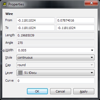
Our lengths look really weird because this line was drawn in metric and is being converted to inch. Let’s modify this to -0.0965".
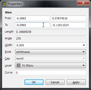
Repeat for the right bar with 0.0965”.
Whoa. This IC is getting smaller!
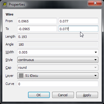
Now let’s modify the top bar and bottom bar to be 0.154" / 2 = 0.077"

Ahh! We now have the physical outline of this SSOP package. It’s small!
Time to save your work. Click on the disk icon or hit Ctrl+s.
When dealing with IC dimensions have a calculator handy and be ready to convert between metric and imperial (I’m lazy and use google). If you don’t have a datasheet for your part, don’t fret! Get the part in your hand, pull out your digital calipers and start measuring. We've created many parts without a datasheet.
Now we need to add SMD pads around this outline. From the datasheet, each pad is:
- 0.041” long : (dimension E - dimension E1) / 2
- 0.01” wide : dimension b
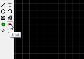
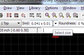
Click on Smd (come on Eagle! It’s SMD not Smd!). You’ll have a red rectangle floating around. Now go up to the Smd: box and enter 0.041x0.01.
Now wait! We have created a pad that is exactly the size of the pin. We actually want a pad that is slightly longer and slightly wider than the pin so that we can have solder fill around the pin and the pad. I will sometimes increase by ~10-20% in each direction. There is no hard and fast rule here. We often find recommended footprint datasheets for similar footprints. For this example, I’m going to look at the SSOP20 footprint contained within the Digital ICs library and use the pad dimensions for that component. I know SSOP20 works well (we've used the old FT232 IC many times) so I trust that pad size.
Click on the Package button in the top menu within the Eagle window then scroll to SSOP20.
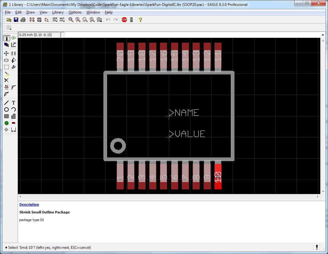
Click on the ‘i’ (not the eye ball) and click on a pad. Make sure the red pad is highlighted and not the white pad. If the wrong pad is highlighted, right click and Eagle will cycle through the items that are stacked upon each other.
0.01574803 x 0.05905512 ?!? What the heck is that? Remember, we are on the imperial grid. Let’s close this window and hit Alt+F10 to switch to the metric grid. You should see the grid change in size. Now click on the same pad. If the white block gets highlighted hit escape (to close the pad information window) and trying clicking on the more central location of the red pad.
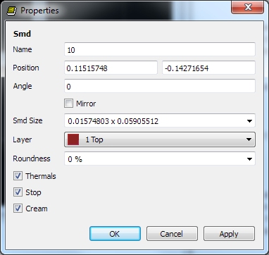
0.4 x 1.5 - Ahah! This makes a lot more sense. The pad was created on the metric grid. Let’s do the same for our component. Remember this value.
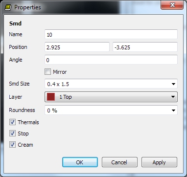
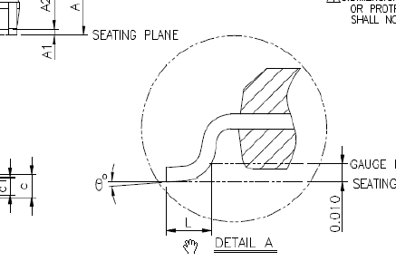
Before we leave this package, let’s talk about the tDocu layer and why there is a white square on top of the red square. Remember how we said we needed to create a pad that is bigger than the pin? The person who created this package created a white square to indicate the actual pin on the top document layer (tDocu) and an actual electrical pad using the Smd button. This allows the engineer to see where exactly the pin is located and where the SMD pad is located underneath. This white pad is really just there to help us visualize everything going on. Also note that the red pad is not concentric (does not share the same center point) as the white square.
(picture of pin on pad at angle)
This is because only part of the pin hits the pad. This is dimension L on the datasheet:
This is all pretty minute details to creating the pad for this device. For your own SMD package remember:
- Create a SMD pad that is slightly larger than the pin dimensions
- Locate the pad so that it is near the center of where the metal pin will be
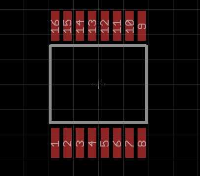
Ok - now let’s return to the new SSOP16 footprint we were creating. Click on the ‘Package’ button located in the top Eagle menu, scroll down to the SSOP16 package and double click it. You should now see the white box we created.
Click on SMD and create a pad that is 0.4x1.5.
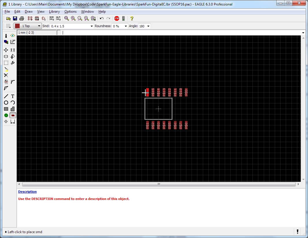
Drop 16 pads (this is a 16-pin device) around the outline of the package.
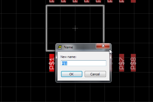
Let's rename the pads to ‘1’, ‘2’, etc as they are labeled in the datasheet (the pin numbers wrap around the device in a counter clockwise fashion).
Press F4 to go into Name mode (or click on the Name button). Then click on the lower left pad. Rename this pad to ‘1’. Goto the next pad and name it 2, and so on.
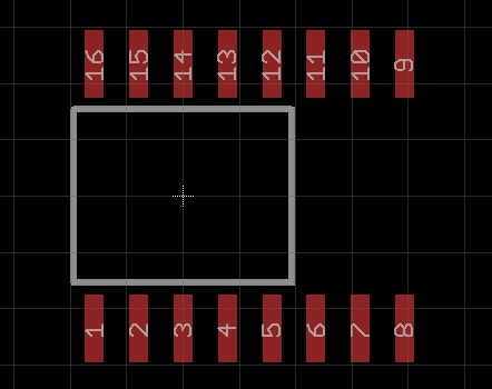
All done. You might be thinking that you should be naming the pads for what they actually do (1 is TX, 2 is RTS#, etc). This is incorrect. We are making a generic SSOP16 package. Later we will associate the pin function with pad #s. For now, just be sure you are number the pins correctly. Connectors are often numbered differently from ICs so read your datasheet closely.
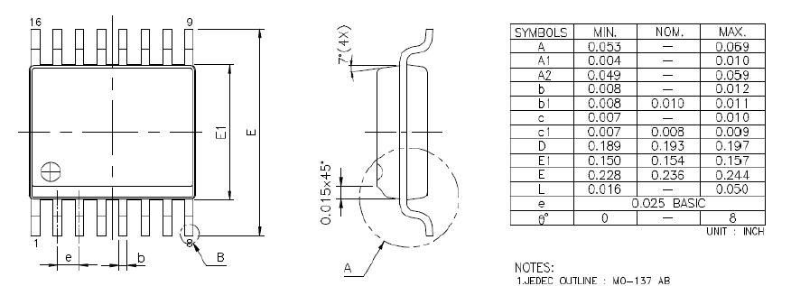
Back on the datasheet, look at the e dimension (little e, not big E). This is the distance between pins, also known as pin pitch. For this IC, the pitch is 0.025”.
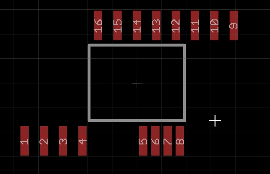
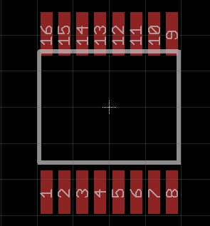
There are 8 pins on each side so I am going to start on the lower row of pads, setting pad 5 at +0.0125” (1/2 of 0.025”). Click on the ‘i’ button, then on Pad 5. Adjust the X location to 0.0125 then click ok.
Pad 6 will be at 0.0125 + 0.025 = 0.0375”. Pad 7 will be at 0.0625, etc. Repeat for pads 5 through 8.
Neat! Those pads are pretty close together but it looks like the spacing is making sense.
Now do the same for pads 1 to 4. Pad 4 will be ½ of 0.025 = -0.0125”. Pad 3 will be -0.0125 - 0.025 = -0.0375 and so on.
You should now have the bottom pads with the correct X coordinates. Now, leveraging symmetry, we can use those same X coordinates and do pads 9 to 16. Click on each pad (I started with 16 and worked my way right) and adjust the X coordinate.
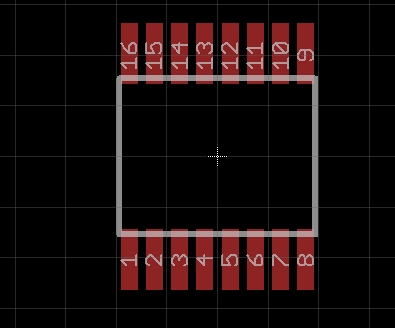
Now we need to calculate and adjust the Y coordinate for all pads. This is a bit tricky, but get the datasheet in front of you and follow along:
We want the SMD pad to be located under the center of pin (metal leg) of the device. We want to find the dimension from the center of the IC to the center of the metal leg. We can infer this from dimension E (0.236”) and dimension L ( MAX 0.05 - MIN 0.016 / 2 = 0.033”).
From the center of the IC to the outside edge of a metal leg is E/2 (0.236 / 2 = 0.118”).
Then we need to come back ½ the width of the metal leg which is L / 2 (0.033 / 2 = 0.0165”).
So 0.118 - 0.0165 = 0.1015”. It is 0.1015" from the center of the part to the middle of each metal leg.
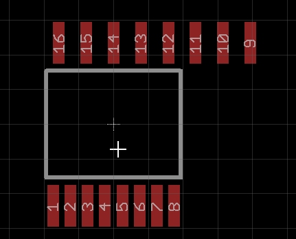
This is the Y coordinate for all the pads on the top row (16 to 9). Let’s adjust them by clicking on ‘i’ then on each pad, correcting the Y coordinate to 0.1015” as we go.
The top row has been adjusted. This looks pretty good. Let’s bring the bottom row up as well.
Time to save your work! Hit the disk icon or hit Ctrl+s.
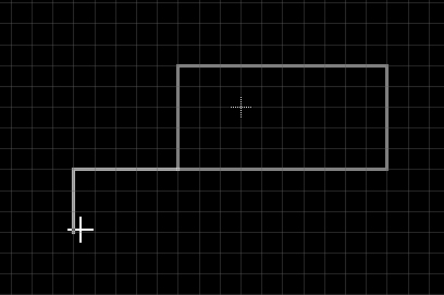
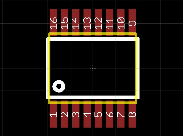
Now let’s check our work. We know the outer dimension of the legs is E (0.236”), so let’s draw a line on tDocu. Click on the ‘wire’ button and draw a line that is a few grids long:

Hit escape to stop drawing. Now modify the Y coordinate of this line (by hitting ‘i’ and clicking on the line) to be 0.118 to -0.118. This line now represents the exterior edge of the pins on the actual IC. Press F7 to go into ‘move’ mode. Then click on the line you just created. Now you should be able to move this line around.
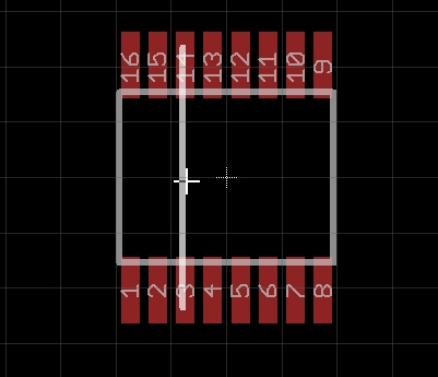
The line will jump around on the major grid. To go to the alternate grid, press and hold the ‘alt’ key as you move the mouse. The line should move with much more fine adjustment now.
We’re using the line as a measuring stick to see where the edges of the pins will fall on the pads. Does it look like the edge of the pins will fall towards the middle of the pads? Yep. Looks pretty good to me. Move the line somewhere off to the side and click once to drop it there. Now hit F3 to go in to ‘delete’ mode and click the line to delete it.
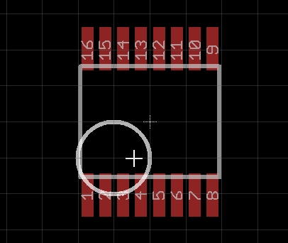
Let’s add a pin 1 indicator by clicking the 'circle' button. The last time we drew anything it was on the tDocu layer. We want this indicator to appear in the silkscreen on the PCB so that we know how to orient the IC on our board. So before we start drawing, click the scroll wheel of your mouse to bring up the layers window and select tPlace (top placement is the silkscreen layer on the PCB).
Now move your cursor in the bottom left corner near pin 1 and click once. What the?! Eagle is trying to snap to the major grid. That’s bad. Hit escape to cancel this drawing. You should still be in circle mode. Hold the alt button, move your cursor where you want the center of the circle and click once then move your mouse cursor.
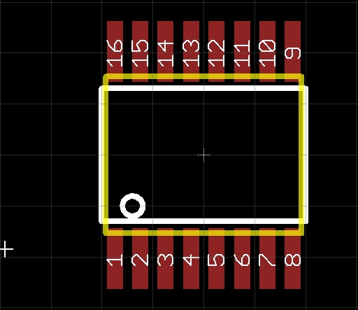
Ahah! The circle is now where we roughly want it. Notice that the tPlace layer (which will get printed) looks identical in color to the tDocu layer (which is only used for reference and will not get printed on the PCB). Confusing! So let’s fix this by modifying the layer colors. Click on the ‘display’ button located on the left menu bar under the 'i' button.
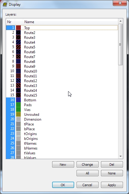
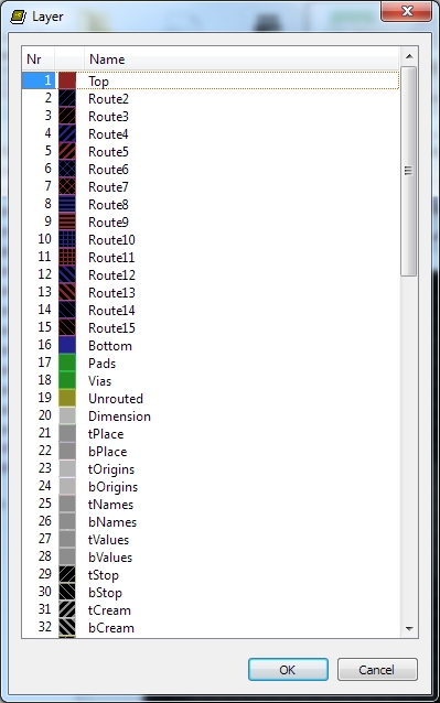
Here we see a multitude of layers. I am going to delete layers Route2 through Route15 because I have never created a footprint that had interior layers. You may want to leave them if you’re a super user.
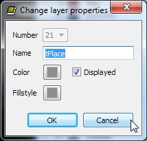
Double click on tPlace. Then click on the gray square next to Color. Change the color to white. Click on ok to back out to the layers window.
Now let’s change the color for tDocu. Change it to mellow yellow.

Ahh! That’s a bit easier to visualize what’s going on. White will be silkscreened. Yellow is just there so we know where the IC edges are. I prefer to have a white box one my PCB indicating where an IC goes so let’s draw some lines on the tPlace layer.
Here I’ve made a white box, slightly longer than the tDocu lines and slightly skinnier. This will prevent me from putting anything too close to the end of my IC, possibly hitting a nearby component. However, there is a problem with this. Silkscreen should have a thickness of 0.008” or larger so that the PCB fab house can print it legibly. Trying to print too small of silkscreen will cause line to flake off and turn text into white blobs.
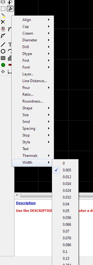
So let’s modify this silkscreen width to be 0.008” by clicking on the ‘Change’ wrench, then ‘Width’ then the ‘...’ at the very end of the list. You’ll get a window where you can enter your own width. Enter ‘0.008’ and press enter. Any line you click on will now change to 0.008”
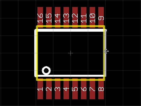
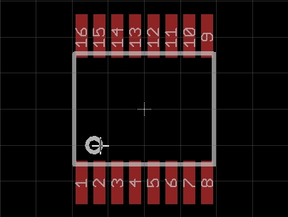
Click on each white line increasing its thickness. Also click on the pin 1 indicator circle. The circle is now kind of close to the edge so let’s move that up and over a bit. Do so by hitting F7 to go into move mode. Click on the middle of the circle. It will want to snap to the major grid so hold alt down while you move the circle and it will give you more fine placement.
The final thing to do is add a ‘>Value’ and ‘>Name’ text tags on the tValues and tNames layers respectively. Eagle looks for these special tags and populates them with the value and name of the IC when you’re in PCB layout mode. Eventually, we will see ‘FT230X’ and ‘U3’ automatically populated here.
Click the ‘text’ button. Eagle will prompt you for the text. Type >Value and press enter. Before placing the text, click your scroll wheel and select the tValues layer.
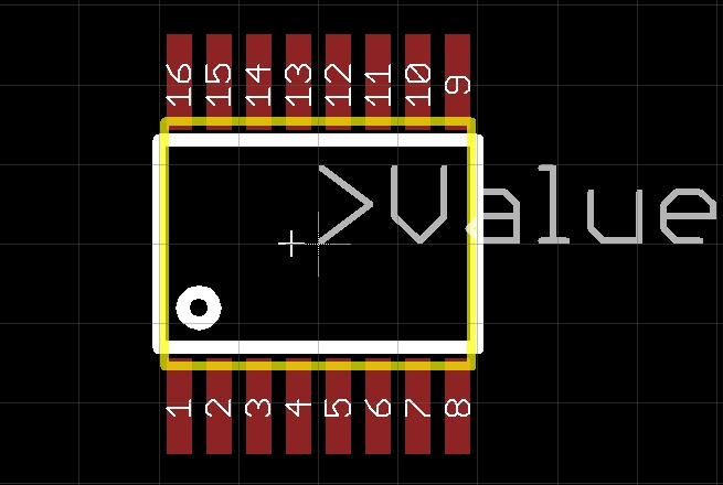
As you move around, you'll see that this text is a bit large so I am going to change the size to 0.025. Find the Size box in the top menu bar. Type 0.025 and press enter.
Now place the text in the middle of the IC by holding the alt button (to get finer grid). Once you’re happy, left click once to place the text. Hit escape. You’ll be returned to the ‘Enter text’ window. Hit escape a second time to return to the main window. Now repeat the process but this time with >Name and place it on the tNames layer.
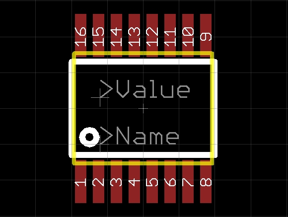
Looking really good! Be sure to give some sort of description to your package. Do this by clicking on the blue ‘Description’ line at the bottom of your screen. Eagle will bring up a window that allows you to edit this package’s description.
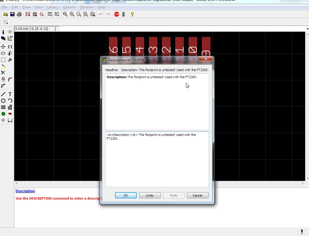
I like to put information about what component this package goes with. In our case, we’re creating this package for the FT230X but it could be used for other SSOP16 sized ICs. I also like to mention when this is a new/untested footprint or when it has been fully tested. The problem with this is that I often forget to come back and update the package description so do what you wish. Save your work!
Congratulations! You’re done with creating the SSOP16 package! Now let’s create the schematic symbol.