Designing PCBs: SMD Footprints
 Nate
Nate 
Device Creation
Eagle requires three things to get an IC into the library:
- Package (also known as a footprint)
- Symbol (the schematic symbol)
- Device (mapping them together)
The tutorial images show us working from the SparkFun-DigitalIC.lbr file but you can create your own custom library file if you'd like.
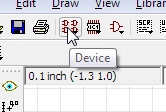
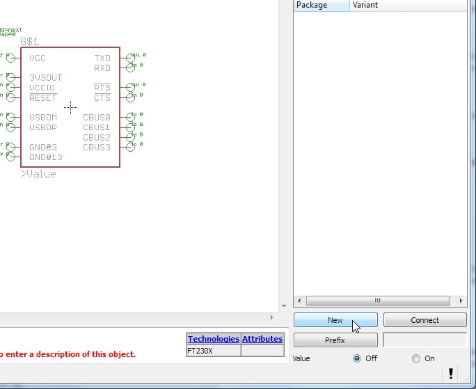
It’s time to create a device. The device maps the make-believe schematic symbol to the real-world footprint. Start by clicking on the device button.
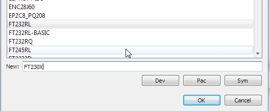
It’s always good practice to check to see if we already have a device created. From the device list you can see that we do not currently have anything like the FT230X device, so let’s create a new one.
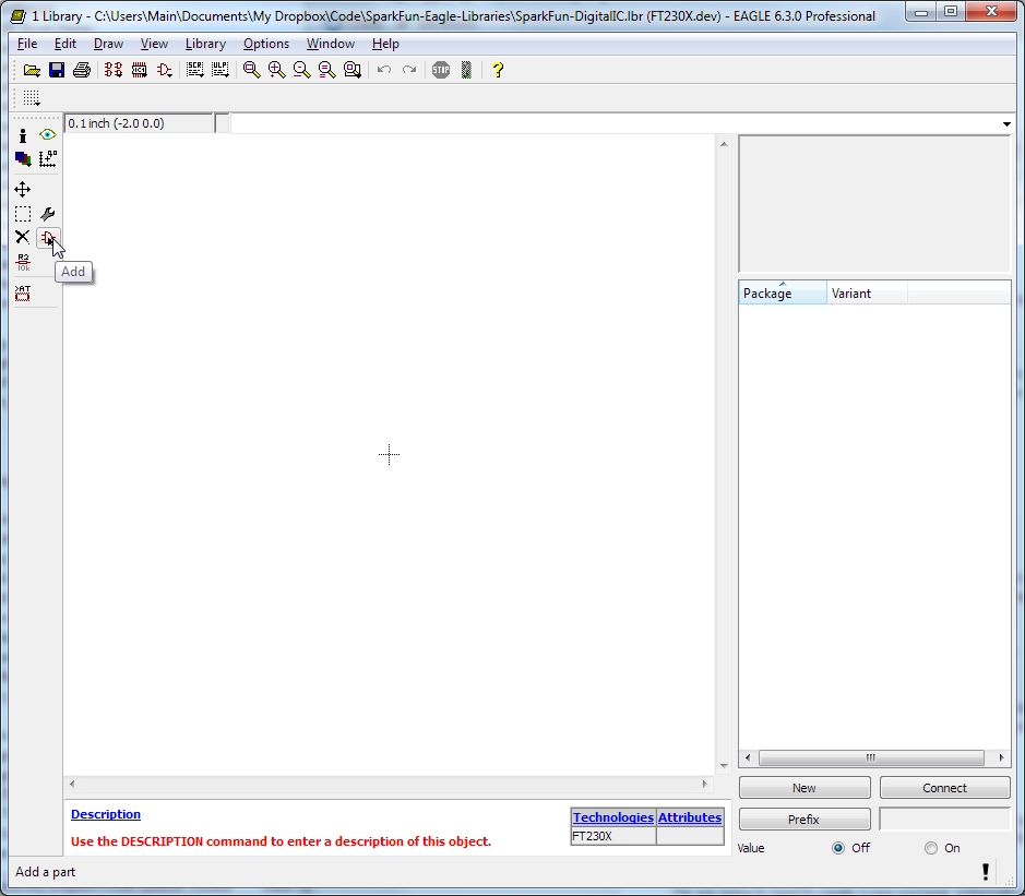
First step, click on ‘add’ to add the schematic symbol to your device. Navigate the list of symbols until you find the ‘FT230X’ you created earlier. Double click it.
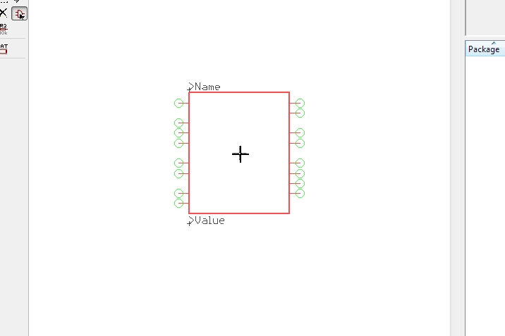
Drop your symbol so that the center of the symbol aligns with the center of the device space and left click your mouse. Hit escape twice to exit back to the main window.
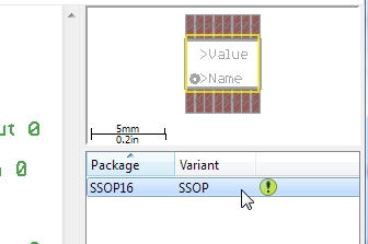
Now click on ‘New’ package. Navigate to the SSOP16 package you created earlier and double click.
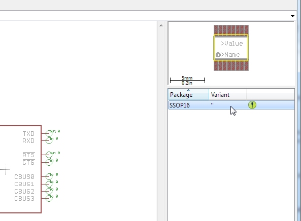
In the main window you’ll see a new package with variant labeled “ (this is the default) and an exclamation point.
A given integrated circuit may be pacakged in a varienty of different shapes and sizes (for example DIP, SSOP, or smaller QFN type packages). The variant name allows you to have multiple footprints for the same schematic symbol.
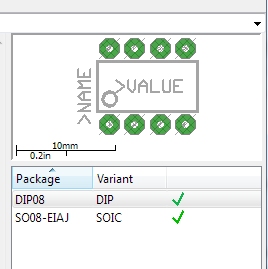
The ATtiny shown above is a good example. The IC is the same but it comes in two different footprints: 8 pin DIP and 8 pin SOIC. You cannot have a duplicate variant name so in this example we used 'DIP' and 'SOIC'.
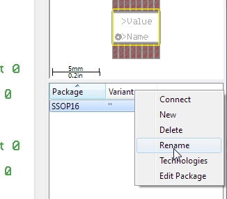
Eagle will not allow you to have two packages with the same variant name. To change the variant name, right click on the package type and click ‘Rename’. Give this package a name such as SMD or DIP or SSOP. Whatever you need to make it clear what package variant this is.
Next we need to tell Eagle what pad on the package goes with which pin on the symbol. Double click the bar under the package window, or click on the button ‘Connect’ at the bottom of the window.
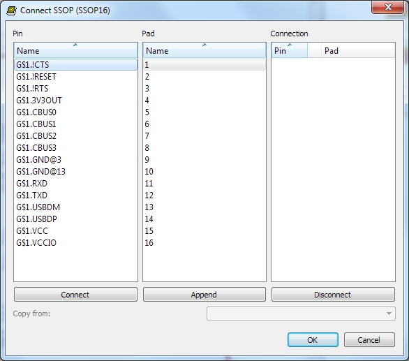
This is a very important step. We must refer to the datasheet for the FT230X and be very careful to correctly connect the pins and pads correctly. CTS is pad 4 so with CTS highlighted, double click on 4 in the pad list.
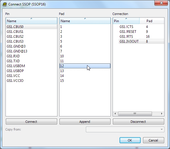
Continue until you’ve connected all the pins to the pads. If you have pins left over, that’s bad and Eagle will complain. However, if you have pads left over, that’s ok - you probably have some pads on the footprint that are left unconnected.
If you do have anything left over, this is a good time to double check that you’ve correctly identified all the pads and pins on your footprint and schematic symbol correctly.
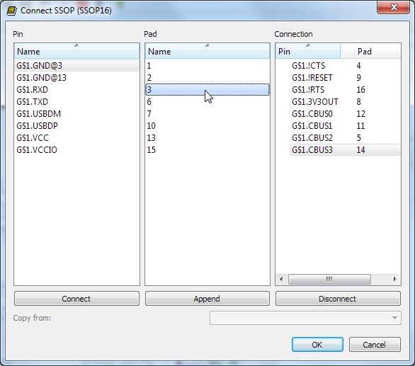
Remember when we named the pins GND@3 and GND@13? Guess which pad GND@3 connects to? Pad 3! And GND@13? Pad 13! This is why we used that @ sign - to make it easier when we have multiple pins of the same name to connect to different pads.
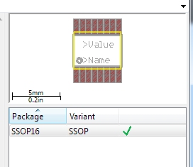
Once you’re done you should have a nice green check mark next to your variant.
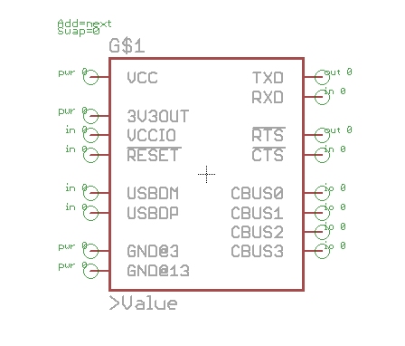
Note the G$1 over the symbol. The ‘G’ is wrong for integrated circuits (we normally use ‘U’) and the ‘$’ is super annoying and looks bad on the schematic. To get rid of this, click on the ‘Prefix’ button in the lower right corner and type ‘U’ with nothing else. This will make the default prefix ‘U’ instead of G$. Upon returning to the main window the G$1 will still be there. To change that, press F4 and click on the symbol. You can then change the name to U1.
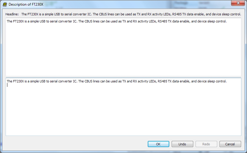
Be sure to give a good, lengthy description of your device! It will help tremendously when you have a library of 100 different parts. Now save your work!