Understanding Thermal Resistance
 Alex the Giant
How to Transfer Heat
Metal Fin Heatsinks
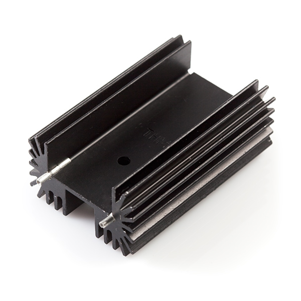
Heatsinks some in all shapes and sizes, with a single purpose: transfer heat to the air. The purpose of each of the fins on a heatsink is to create as much surface area as possible for the air to interact with and pull heat away from the heatsink, which helps to pull heat away from the semiconductor’s junction. The thermal resistance of a heatsink can be a bit complicated though because a metal fin heatsink performs at different rates based on the amount of air flowing past the fins. A typical datasheet for a heatsink provides not only the dimensions of the part, but the thermal characteristics as well, which looks like this:
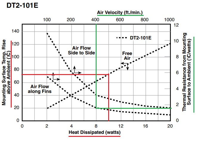
The arrows on each plot line correspond to the axis they represent. For example, the red highlight shows that in free air (ie without a fan), dissipating 10W of power would raise the temperature of heatsink around 78°C above ambient temperature. If instead you had around 400ft/min of air flowing along the fins of the heatsink, the green line shows the heatsink would have a thermal resistance of around 1.8°C/W, or 18°C above ambient temperature dissipating the same 10W of power.
Vias
If you need to add a heatsink to the design, designs like switch mode power supplies where it’s important to keep components as close to the IC as possible, vias can not only transfer signals from one side of the PCB to the other, but they can transfer heat too!
If you don’t feel like doing a bunch of math, the PCB Toolkit from Saturn PCB Design Inc has a lot of great tools to solve a ton of the equations an electrical engineer might use. One of the tabs in particular is for via properties:

To get the thermal resistance of the vias, I entered in the boxes I highlighted red the properties of the PCB I have. Setting the layer set to 2 layer, and the via hole diameter should be the only setting you might need to change. The via plating thickness and via height are pretty standard for most PCBs. After clicking solve, in the blue box in the bottom right corner I got the thermal resistance which was 179.3°C/W per via. With 10 vias, the via thermal resistance drops down to 17.9°C/W. If you were going to calculate the junction temperature now, you would add another thermal resistance in series for the vias, which would be added with the other thermal resistances when you do the calculation.
PCB Heatsinking
When it comes to transferring heat in a PCB, the math can get complicated pretty quickly, which is one of the reasons why for via thermal resistance, using the tool from Saturn PCB is the easier way to go. Even more complicated is using a PCB as a heatsink. There’s the thermal resistance not only of the copper, which is a function of the surface area, but the solder mask, substrate material, which also transfers heat to surrounding isolated copper planes. For a thorough explanation, you can read this application report from Texas Instruments. For easier to digest information, Paul Bryson has a great blog post on the subject and provides some great tips and findings which can be found here.
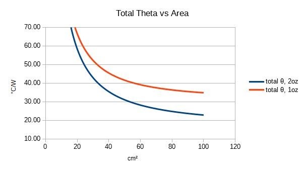
For a rough guide you can use the graph from Paul Bryson's post below: