SparkFun Pro nRF52840 Mini Hookup Guide
 jimblom
Hardware Overview
With the nRF52840 overviewed, let's take a quick look at the features of our board equipped with the Cortex-M4/BT SoC:
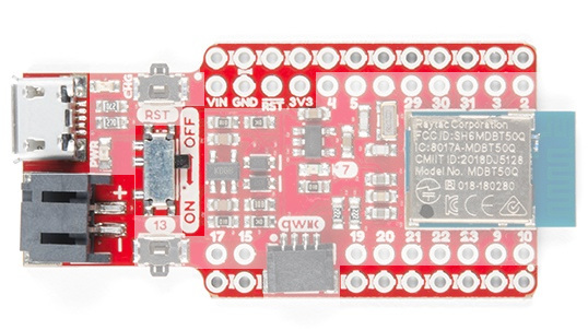
Raytac MDBT50Q-P1M Module
The Pro nRF52840 Mini Breakout actually features a Raytac MDBT50Q-P1M module. This module connects the nRF52840 to an trace antenna, fits the IC into an FCC-approved footprint, and also includes a lot of the decoupling and timing mechanisms (i.e. 32 MHz crystal) that would otherwise be required for a bare nRF52840 design.
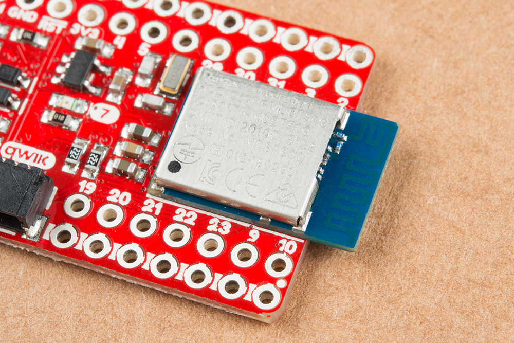
For more information on the MDBT50Q-P1M, check out the datasheet.
SparkFun Pro nRF52840 Mini Pinout
Most pin breakouts on the SparkFun Pro nRF52840 Mini are general purpose I/O pins (GPIO). As mentioned in the last section, GPIO on the nRF52840 can be muxed to just about any functionality your project requires.
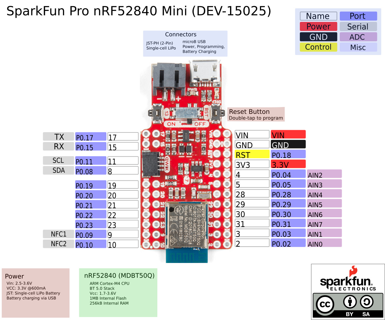
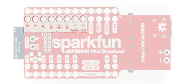
The analog-to-digital converter (ADC) pins are the only ones you may need to put extra focus on. These pins are broken out and available on GPIO pins 2-5 and 28-31. You'll find these pins on one side of the board; they're helpfully highlighted on the bottom-side silk.
The footprint of the SparkFun Pro nRF52840 Mini nearly matches that of the SparkFun Arduino Pro Mini. You'll find power pins in the expected spot. And GPIO — aside from those covered by the qwiic connector — can be used for any purpose (UART, I2C, SPI) that those of the Arduino Pro Mini could.
There are breakouts for the 3.3V regulator output (3V3) and input (VIN). Check out the next section for more information on these pins.
Finally, you'll find an array of ground breakouts on the outside edges of the board. These are covered -- as well as the board fab will allow -- with white silkscreen.
Powering the nRF52840 Breakout
The breakout's micro-B USB interface can be used to both power and program the breakout. The supply-end of your micro-B cable can be either a computer or a USB wall-adapter.
The nRF52840 consumes a very low amount of power -- less than 20mA on normal, radio-transceiving operation. Any computer USB interface should be able to reliably power the module.
Alternatively, the nRF52840 Mini breakout's 3V3 and VIN pins can be used to directly power the board. Power to the VIN pin should be regulated to somewhere between 3.3V and 5.5V, as this supplies the low-dropout 3.3V regulator. If you want to bypass the regulator, a voltage between 2.5-3.6V can be applied to the 3.3V pin to supply power to the nRF52840 module.
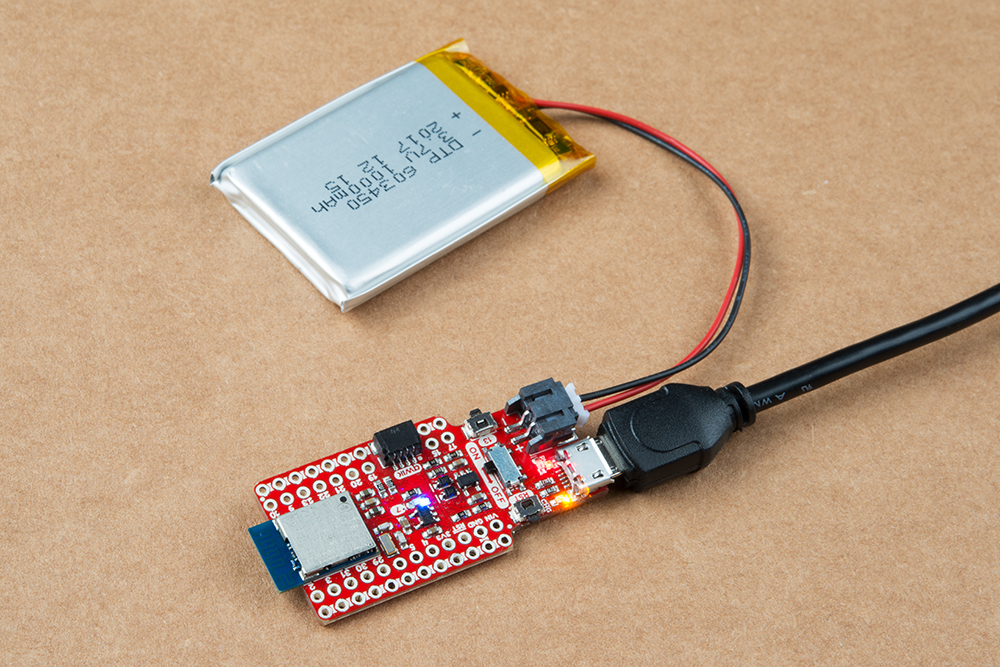
LiPo Charger
In lieu of (or in addition to) the USB supply, a Lithium-Polymer (LiPo) battery can be used to supply the breakout.
A smart-power-selection circuit will ensure that if both USB and LiPo are connected, power to the nRF52840 and its components will be supplied by the USB interface, otherwise LiPo power will be used to supply the system. The USB interface can also be used to charge the LiPo.
ON/OFF Switch
An SPDT on/off switch is populated on the board. This switch controls the enable input on the 3.3V regulator, so any power supplied on the VIN-side of the board (USB and LiPo included) will be regulated by this switch.
The switch, initially, seems oddly placed toward the inside of the board. This helps maintain the small form-factor and ensures spurious swats don't accidentally cycle your project's power.
If you can't get a fingernail into the narrow gap between the switch and components, a pair of tweezers may do the trick.
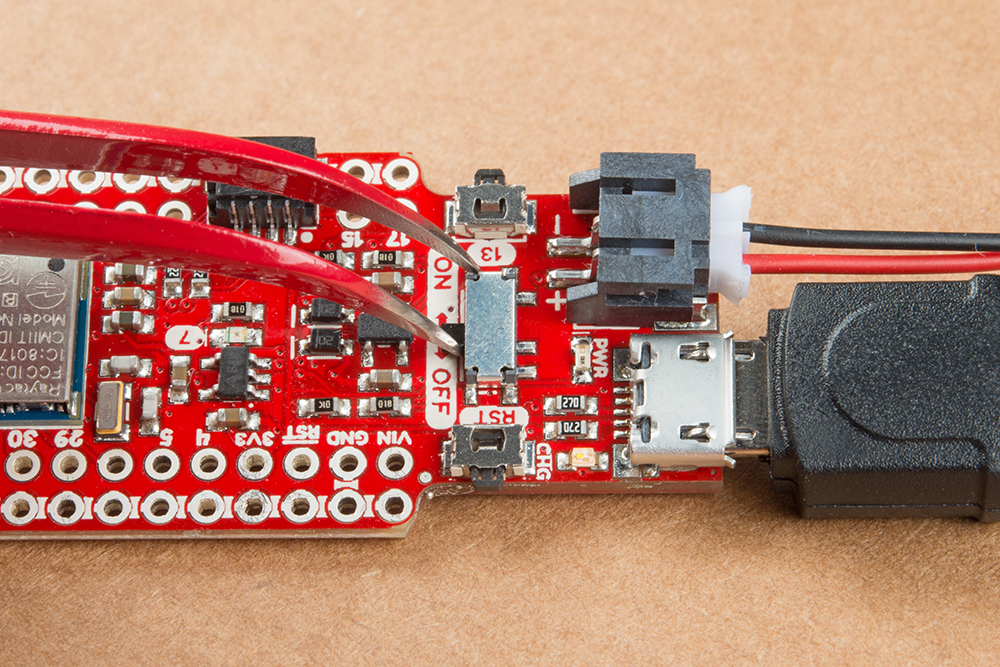
Reset and Pin-13 Buttons
Reset and user-programmable momentary SPST buttons are provided on either sides of the on/off switch. These buttons play a critical purpose in triggering the bootloader, which we'll delve into more in the next section. In your application, the pin-13 button can be used for any purpose.
Both of these buttons are pulled high, so their signal will go low when the button is actuated.
LEDs: Power, Charge, and Pin 7
The board is equipped with three LEDs. Their color and feature-indications are:
| LED Label | Color | Purpose |
|---|---|---|
| PWR | Red | 3.3V power indication. Inidicates the nRF52840 is powered. |
| CHG | Yellow | LiPo battery charge indicator. Illuminates when the battery is charging. |
| 7 | Blue | nRF52840 pin 7. Active-high. Will blink in bootloader mode. |
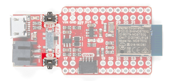
Qwiic Connector
A qwiic connector is provided on the board, with a pair of the nRF52840's I2C-capable pins connected to SDA and SCL.
The nRF52840's P0.11 pin is connected to the qwiic connector's SCL and P0.08 is connected to SDA. See the pinout image here for quick reference.
 |
 |
| Qwiic Connector | Qwiic Connector Pins P0.11 and P0.08 |
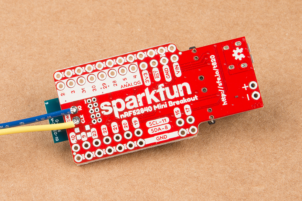
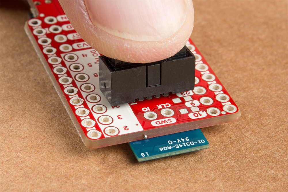
SWD Interface
If you ever want to bypass the bootloader (or knock-on-wood you brick it), the nRF52840's single-wire debug (SWD) pins are broken out on the bottom of the board.
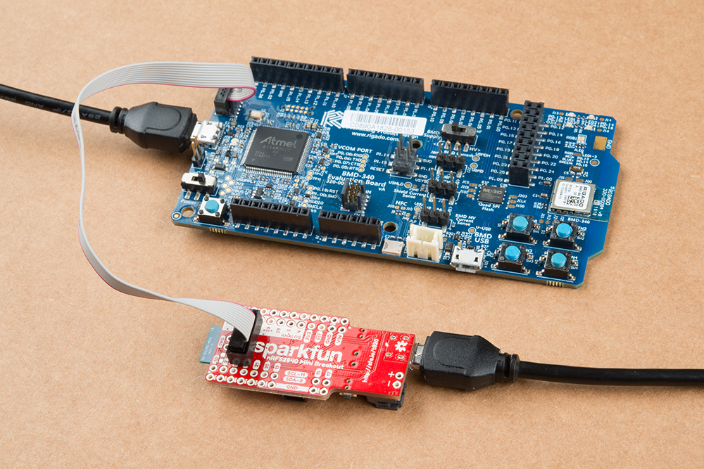
They may be difficult to solder to, as the module blocks the other side, but they can be held in place while you quickly program. A 10-pin, 2x5, 0.5" pitch header, for example, can be angled, and pressure-fit into the 10-pin, 2x5 Cortex-debug connector. Make sure you match up the debug cable's pin-1 indicator to the small silkscreen pin-1 indicator on the board! In the following example, a polarized female header was used to connect the cable to the board.
You can then use a programming tool, like Nordic's nRF52840 DK to flash new firmware onto your nRF52840 via SWD.
The SWD's IO and CLK pins can also be soldered to using relatively high-gauge wire, and routed to the programming interface of your choice if you prefer.