RETIRED - Using the Logic Level Converter
This Tutorial is Retired!
This tutorial covers concepts or technologies that are no longer current. It's still here for you to read and enjoy, but may not be as useful as our newest tutorials.
View the updated tutorial: Bi-Directional Logic Level Converter Hookup Guide
 jimblom
Hardware Overview
The LLC is a very simple device. That's apparent when you look at the schematic. Click the image below to get a bigger view of the schematic, or click here to view it as a PDF:
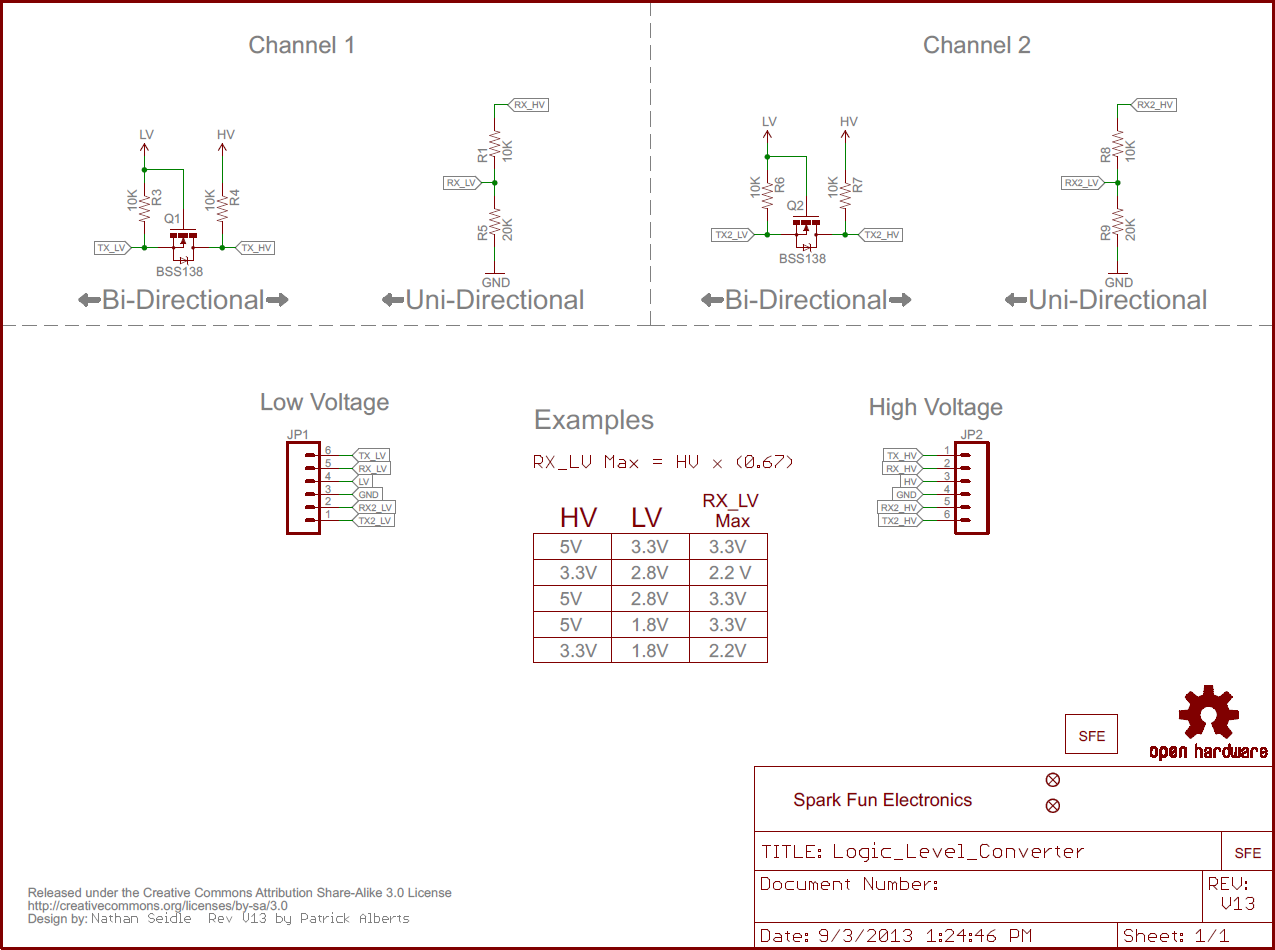
Essentially, there are two different circuits at work here: a voltage divider and a MOSFET-based, bi-directional level shifter.
The voltage divider level-shifting circuits cut a high voltage down by 66%. The voltage divider ratio was chosen to divide a high voltage of 5V down to 3.3V, the most common use case for the LLC. Note that the voltage-divider circuit can't work the other way -- it can't make a voltage higher. That's why we need a different circuit for the other half of the LLC.
Through the magic of semiconductors, the MOSFET-based circuit on the LLC can turn a low-level signal into a higher one. Actually, this circuit has the added benefit of working both ways, it's bi-directional. If one line is pulled low (0V), the MOSFET will be put into a conducting state and the other input/output line will go low too. If both lines are left alone, they'll both idle to a logic high (3.3V, 5V, etc.).
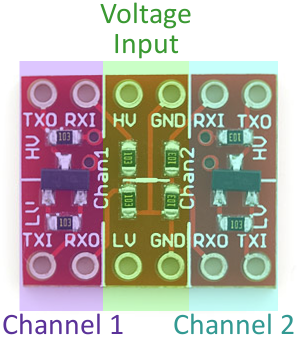
Board Overview
The LLC is designed to be very easy to use. Silkscreen indicators help identify which pins do what. There are twelve pins total -- six on each side. We can divide them into groups of three to more clearly define how they relate:
The middle section of the board is where the reference supply for your high and low voltages should go. Supplying voltage to all four of these pins is required. If you're converting 3.3V to 5V (and vice-versa), for example, you'd run 5V into the "HV" side, and 3.3V into the "LV" input. Make sure each is grounded too!
The outer pins correspond to inputs and outputs for channels 1 and 2. Each channel has one voltage divider and one MOSFET shifter.
The labels on these pins -- "RXI", "RXO", "TXI", and "TXO" -- help describe what each pins does:
- RXI -- High voltage input to voltage divider from high-voltage device. Signal will be shifted down and sent to low-voltage device on "RXO" pin.
- RXO -- Low voltage output from voltage divider to low-voltage device. Signal is shifted down from "RXI" input.
- TXI -- Low voltage input/output of MOSFET circuit. This pin interacts with "TXO" on the high side. Bi-directional, but this is the only shifter that will shift from low to high.
- TXO -- High voltage input/output of MOSFET circuit. This pin interacts with "TXI" on the low side. Bi-directional, but this is the only shifter that will shift from low to high.
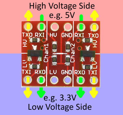
To send a signal from the low-voltage side to the high-voltage side (e.g. from 3.3V to 5V), the signal must be input at "TXI". It'll pass through the converter and come out as a higher voltage on the "TXO" (transmit output) pin.
On the other hand, a signal that strictly travels from high to low-voltage should pass from "RXI" to "RXO".
Sending a signal from the high side to the low side is less restricted. We can use either the bi-directional channel or the voltage divider, but we may need to leave the bi-directional channel for converting from low-to-high.
Using this board is probably a lot easier than the length of this page would imply. Let's look at some example configurations next.