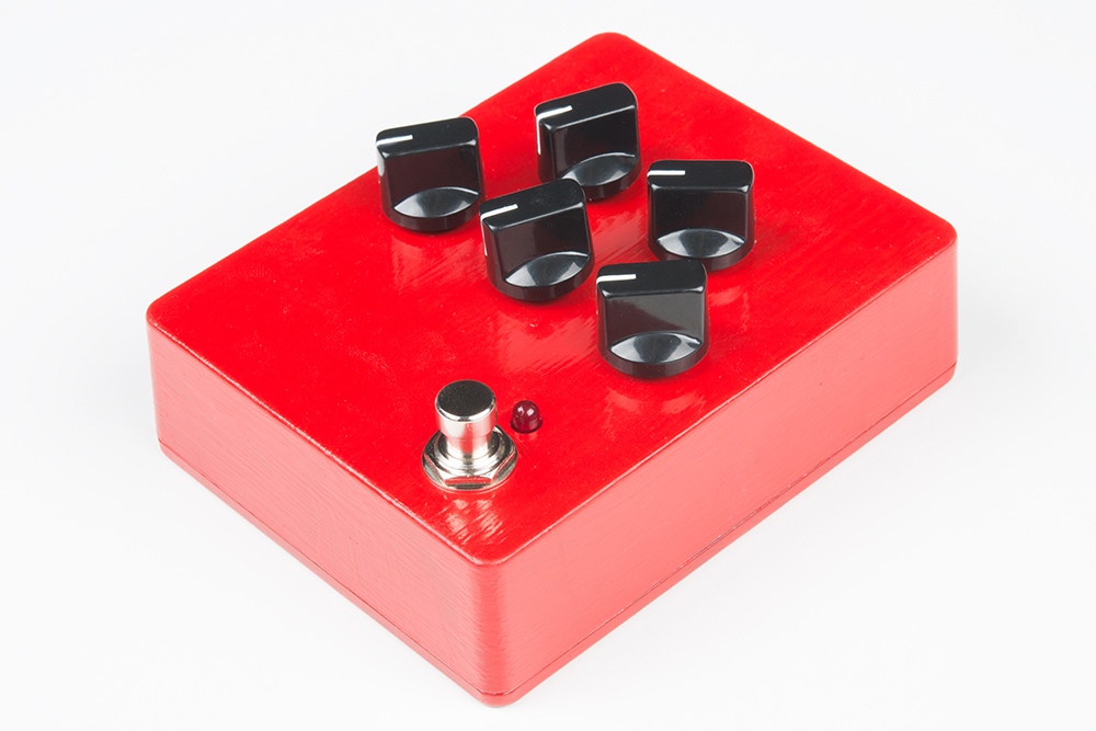
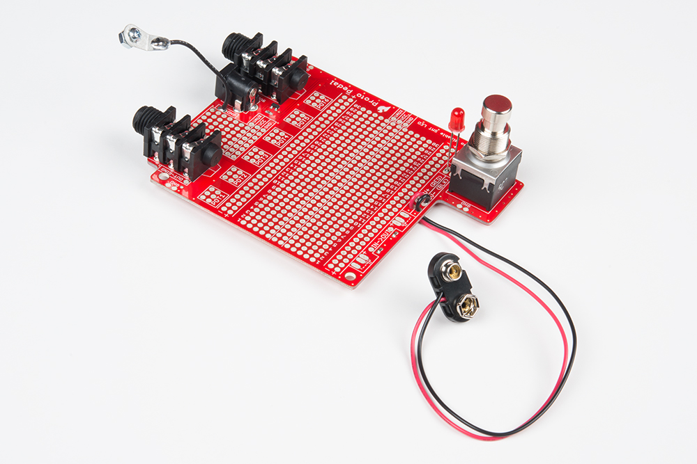
Proto Pedal Example: Programmable Digital Pedal
 Byron J.
Introduction
Having assembled the Proto Pedal in the Proto Pedal Assembly Guide, we’d like to continue by actually building an effect circuit on the board. This time around, we'll be putting a Teensy 3.2 and Audio Adapter in the pedal. The Teensy Audio library contains a bunch of building blocks that you can use to create a custom digital signal processing pedal. Rather than a single effect, you can reprogram the Teensy to create new sound effects.
Suggested Reading
- If you're here, we'll assume that you're familiar with the Proto Pedal Assembly and Theory guide.
- This project also assumes that you're familiar with the Teensy Audio Library.
- In parallel with this guide, you might also be interested in some information about preparing the Proto Pedal chassis.
Background
The Teensy 3.2 is a small board built upon a powerful microcontroller, the Freescale Kinetis K20. It can be overclocked to 96 MHz, and features the Cortex M4 instruction set, which lends itself to signal processing tasks.
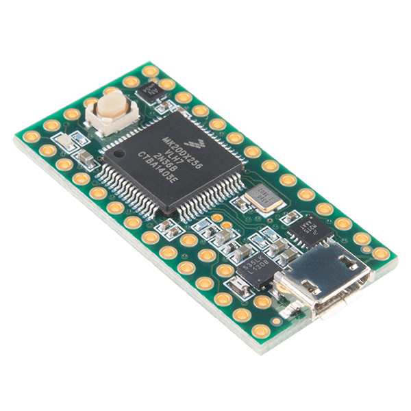
The Teensy is Arduino compatible, and programmable via a USB connection. If you've used any Arduino-based board, you're already partway there.
To help take advantage of the signal processing instruction set, the Audio Board adds a 16-bit stereo audio ADC and DAC.
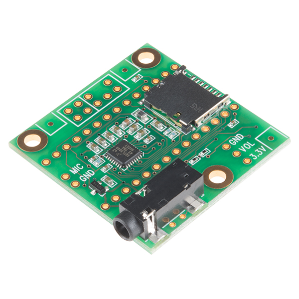
Best of all, you don't need to be a signal processing guru to get started with the audio board. Instead, there's a web based editor that lets you start building the signal processing in a drag-and-drop, patchable GUI. To get started, you assemble the desired processing blocks in the GUI, then cut and paste a snippet of code into an Arduino sketch.
We're going to assume that the reader is familiar with Teensy and the Audio framework. If you need some additional background, there is a guide to getting started with Teensy. PJRC have also prepared a detailed tutorial on the Teensy Audio environment.
In Pedal Form
What were going to do in this project is pair Teensy Audio with the Proto Pedal, resulting a reprogrammable digital guitar pedal.
Before we begin
This is a complicated circuit! It involves a number of different types of wiring -- analog, digital, and power circuits are all included. If you're new to building guitar pedals, this might not be the best starting point.
Second, the noise floor performance of the circuit leaves something to be desired. There's a fair amount of digital crust that the authors have been struggling to remove. If you're a master of noise reduction in mixed-signal systems, we'd love for you to take a closer look! If you find things we have missed in our haste, please inform us using the comments link in the menu to the right, and we can update this guide.
Finally, if you like the idea of this project, but want ready-made hardware, you might see if you can track down the old Line 6 ToneCore development kit.
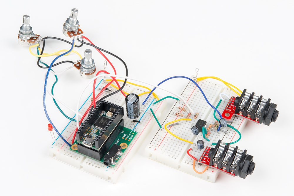
The Circuit
The most important component is in the middle of the schematic: the Teensy and audio adapter. We're using a simplified symbol to represent them, which only shows the connections we're using.
Theory Of Operations
We're going to quickly describe what each section of the circuit does.
Input Buffer
The first portion of the circuit is the input buffer.
It consists of one stage of an LM358 operational amplifier, configured as a voltage follower. It's input is biased to 4.5 VDC with the pair of 1M Ω resistors, and the input signal is coupled to them via the 10 uf cap. The output of the buffer matches the input signal -- the buffer increases the input impedance, but doesn't amplify or attenuate the signal.
It provides a reasonably high impedance of 500K Ω, defined by the parallel 1M resistors. 1M Ω is the highest value resistor in the SparkFun Resistor Kit -- if you've got higher value resistors (such as 2.2 M Ω), they should provide even better performance.
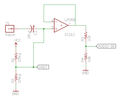
The output of the buffer amplifier feeds the divider of R3 and R4, which attenuates the signal by 10K/(10K + 22K), or 10/32, roughly one-third the input value.
Since this amp stage is powered directly from the 9 VDC supply, it has roughly 9 Vpeak-to-peak overall headroom. Dividing the output by 1/3 constrains it to about 3 Vpp, which more closely matches the input headroom of the Teensy line input that it feeds.
Output Amplifier
The output of the Teensy also has about 3 Vpp headroom, which we amplify back to the 9 Vpp range using an amplifier with a gain of 3.
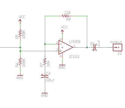
The gain of this noninverting stage is determined by the equation 1 + (Rfeedback/Rshunt), or 32/10, the reciprocal of the attenuation of the input amplifier. This pair of circuits achieve what's known as unity gain, the combined result being a multiply by one. What goes in comes back out the same.
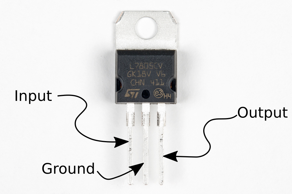
Voltage Regulator
The Proto Pedal operates in a world of 9 V batteries and wall adapters, while the Teensy can operate from a miximum of 6 VDC. To help bridge the gap, we're using a simple LM7805 linear voltage regulator.
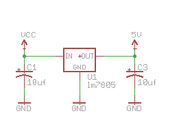
It turns the 9 V into 5 V. The Teensy draws about 60 mA, and the regulator is dropping the voltage by 4 V, so this regulator has to dissipate about 1/4 Watt as heat. It gets a little warmer than room temperature, but doesn't get appreciably hot.
The Teensy has further onboard regulators, dropping the 5 V down to 3.3 V.
Analog controls
Finally, there are five potentiometers, wired as voltage dividers between Teensy 3.3V and AGND.
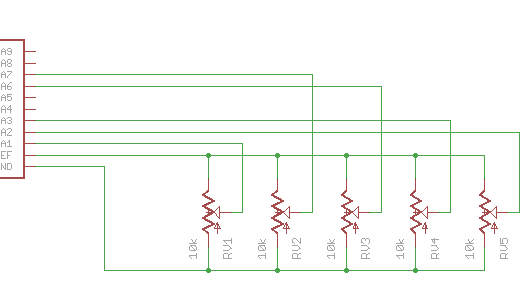
The wipers of these pots are connected to Teensy ADC inputs A1, A2, A3, A6, and A7. These controls can be assigned to effect parameters in firmware, and are not hardwired to specific parameters.
Materials
To build this pedal, you'll need the folliwing materials, in addition to the Pedal PCB and chassis.
Tools
You'll also need the usual tools to solder things together.
- Soldering Iron
- Lead-based or Lead-free solder
- Diagonal or Flush cutters
- Wire Strippers
Additionally, while it's not required, we were using a Resistor Lead Forming tool to get the resistors bent to precise lengths.
Assembly Part 1 (power and analog section)
The Jumping Off Point
To begin, we'll assume that you've completed the basic assembly of the proto pedal board.
One detail worth noting is that you can likely omit the 9V battery snap. While it's possible to power this pedal from a 9V battery, the Teensy is thirsty for current, and you can expect 6 to 10 hours battery life. An external power supply is highly recommended!
If you're using the Proto Pedal Chassis, you'll need to prepare it by drilling holes for five potentiometers, and holes for programming the Teensy. This is the chassis shown in the Chassis hookup guide.
With the prerequisites complete, you can start the sequence below. We'll build the circuit in four major stages: the voltage regulator, the analog section, the Teensy, and the panel controls. We're going to be stepping fairly quickly. Each step lists the required components, so you can prepare them before you commence. Once they have been placed, double-check your solder joints, and compare your work to the photos. Each of the four stages ends with a short test, to test out the results of that stage.
Grid Notation
In the following steps, we're going to use the grid notation seen on a standard solderless breadboard. From left to right, the columns are numbered 1 to 30, and from bottom to top, the rows are assigned letters from A through J. Any hole in the center of the board can be referenced by number-letter coordinate, such as 27L or 7G.
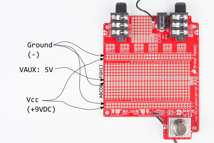
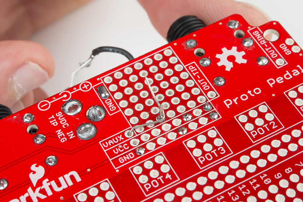
We'll also be using both of the center rails of the proto area. The upper one will be tied to VAUX, the output of the 5V voltage regulator, and the lower one will be tied to ground.
Power Section
Teeny expects an input voltage in the 3.6 to 6.0 VDC range. We'll create a new supply rail for that voltage, using the power section between the input and output jacks, which we'll route to the VAUX trace at the center of the board.
The area near the top of the board has a 7 x 7 grid of pad-per-hole prototying area, plus rails for VCC and ground across the bottom.
We'll start with a LM7805 voltage regulator, and two 10 uf capacitors.
To fit the voltage regulator into this area, we'll bend the legs as follows.
- The output, leg 3, is bent straight down along the body of the regulator.
- The input, leg 1, extends one grid space beyond the body before being bent down.
- The ground, leg 2, is one grid space longer than leg 1.
This contortion is illustrated in the photo below.
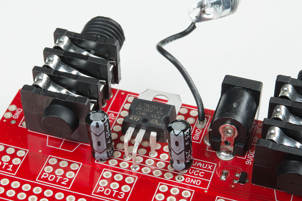
Note the staggered legs of the regulator.
There are also two 10 uf capacitors in this area.
| Capacitor Value | Value Marking | Start Coordinate | End Coordinate | Orientation Notes |
|---|---|---|---|---|
| 10 uf electrolytic | 10uf/25V | Ground rail atfar left | VCC rail at far left | `-` to ground rail |
| 10 uf electrolytic | 10uf/25V | ground rail at far right | VAUX pad at far right | `-` to ground rail + lead extends from VAUX to regulator output terminal. |
The cap on the VAUX rail has a special trick: its positive leg ls run underneath the board, to the output of the voltage regulator, before being soldered in place at both the VAUX pad and the regulator pin. After soldering, trim the excess leads of both the cap and regulator.
Incremental Test
With the regulator and caps in place, we can test the voltage regulator.
Apply 9V power to the board, connect a TS jack to the input, and measure the VAUX pin. It should be in the range of 4.9 to 5.1 VDC.
Before moving on to the next step, be sure to remove power from the unit.
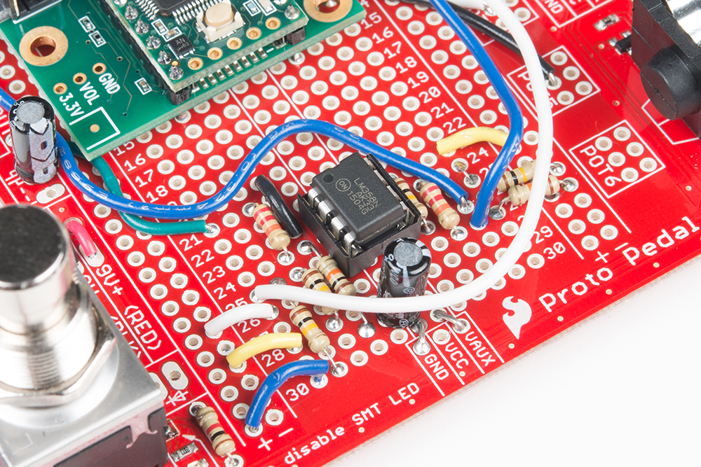
Analog Section
With the regulator tested, we can move on to the analog portion of the circuit. We'll start by placing a bunch of jumpers, then add resistors and caps, finally the IC.
Jumpers
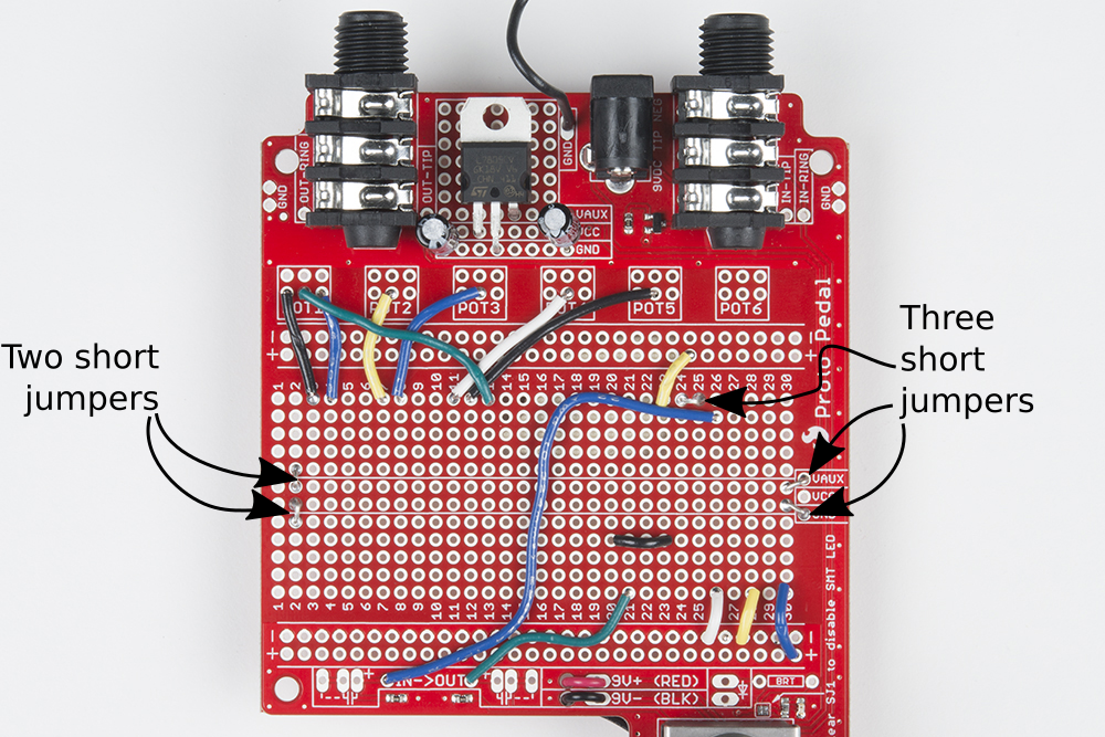
The analog section of the circuit has nineteen jumpers. We used multicolored solid-core 22 gauge wire. For clarity in the photos, we're not using any red wire.
| Jumper Number | Color | Start Coordinate | End Coordinate |
|---|---|---|---|
| 1 | Black | 3J | Pot1 Left |
| 2 | Blue | 4J | Pot1 Right |
| 3 | Yellow | 7J | Pot2 Middle |
| 4 | Blue | 8J | Pot3 Middle |
| 5 | White | 11J | Pot4 Middle |
| 6 | Black | 12J | Pot5 Middle |
| 7 | Green | 13J | Pot1 Middle |
| 8 | Yellow | 23J | VCC |
| 9 | White | 26A | Ground |
| 10 | Blue | Input | 26I |
| 11 | Green | 21A | Out |
| 12 | Black | 21D | 23D |
| 13 | Yellow | 28A | Ground |
| 14 | Blue | 30A | Vcc |
| 15 | Bare | 2F | VAUX |
| 16 | Bare | 2E | Ground |
| 17 | Bare | 24J | 25J |
| 18 | Bare | VAUX | Top Center Rail |
| 19 | Bare | Ground | Bottom Center Rail |
With the jumpers in place the board will look like this
(Click to enlarge).
R's & Cs
Next we'll install the passive analog components, the resistors and capacitors.
There are eight resistors. Most are folded to 0.3" long, with the legs bent right at the ends of the body. One 10K and one 100K are 0.5" long, as noted in the placement column below.
| Resistor Value | Value Color Code | Start Coordinate | End Coordinate | Placement Notes |
|---|---|---|---|---|
| 1M Ω | brown-black-green-gold | 26J | Upper Ground | |
| 10K Ω | brown-black-orange-gold | 27J | Upper Ground | |
| 22K Ω | red-red-orange-gold | 24H | 27H | |
| 1M Ω | brown-black-green-gold | 23G | 26G | |
| 22K Ω | red-red-orange-gold | 21C | 24C | |
| 10K Ω | brown-black-orange-gold | 24D | 29D | 0.5" long |
| 100K Ω | brown-black-yellow-gold | 25C | 28C | |
| 100K Ω | brown-black-yellow-gold | 25B | 30B | 0.5" long |
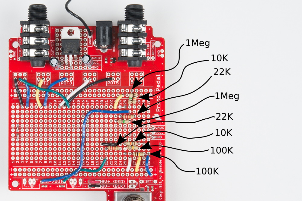
(Click to enlarge).
There are three 10 uf electrolytic capacitors. Take note of the polatiry - the negative leg is marked on the body of the cap with a stripe, which is also visible in the photo below.
| Capacitor Value | Value Marking | Start Coordinate | End Coordinate | Orientation Notes |
|---|---|---|---|---|
| 10 uf electrolytic | 10uf/25V | Input Coupling | `-` to left | |
| 10 uf electrolytic | 10uf/25V | 29E | Center ground | `-` to top |
| 10 uf electrolytic | 10uf/25V | Output Coupling | `-` to right |
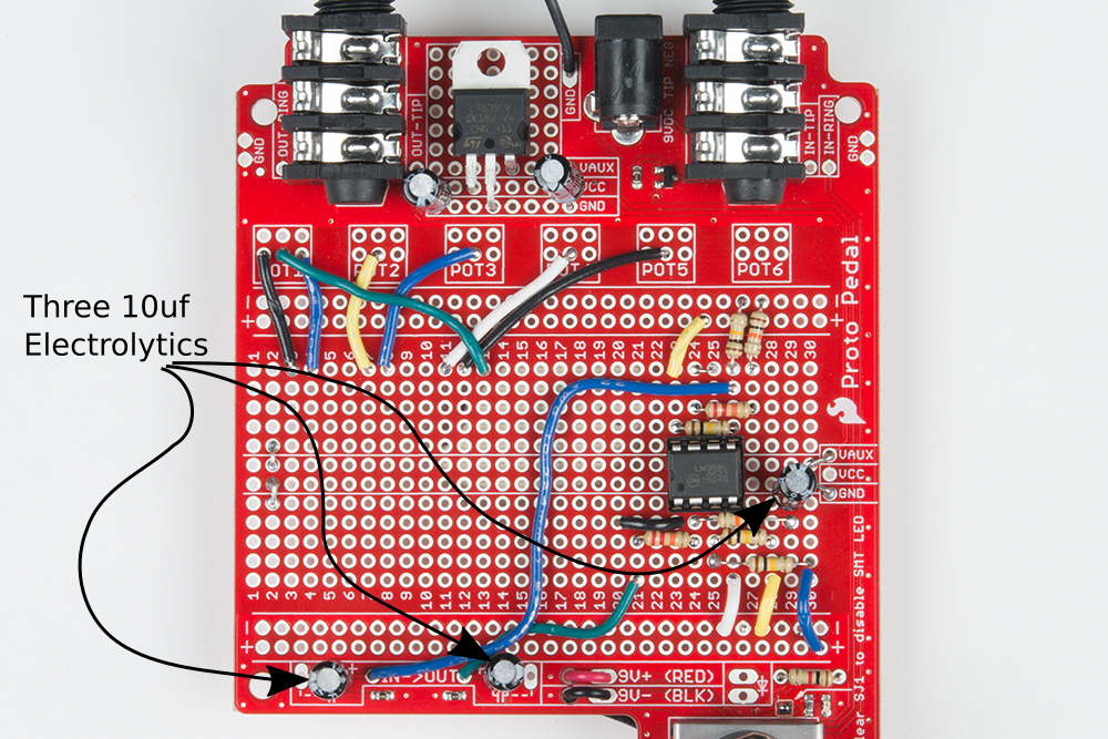
(Click to enlarge).
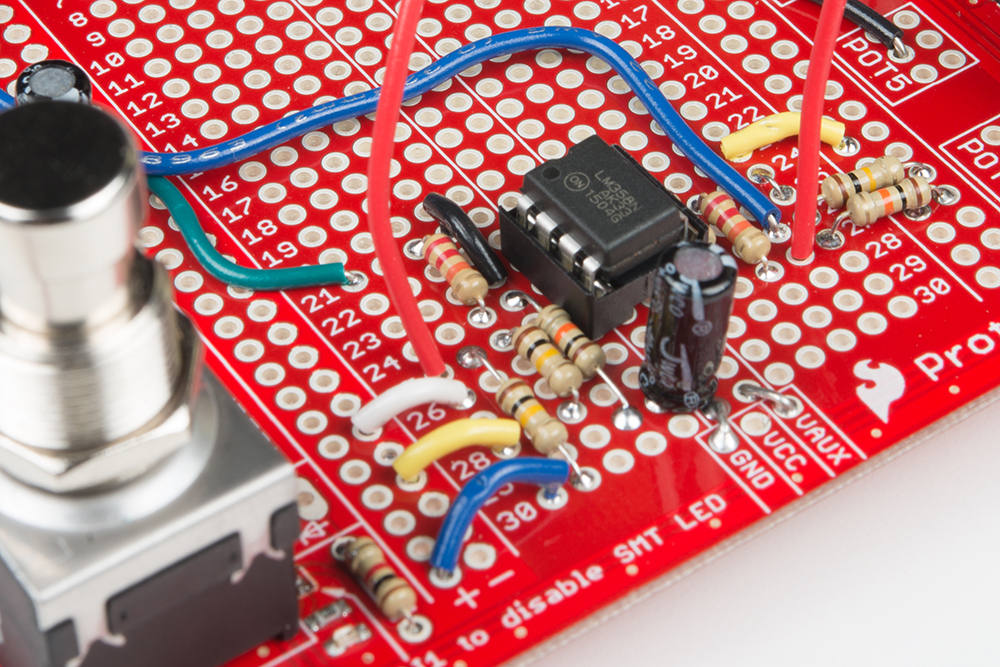
Op-amp
The last component in the analog section is the operational amplifier.
| Component | Marking | Start Coordinate | End Coordinate | Orientation Notes |
|---|---|---|---|---|
| DIP-8 IC Socket for LM358 | Row 23 | Row 26 | Spanning center trough Notch facing left |

(Click to enlarge).
After soldering the socket, insert the LM358, again with the notch facing to the left.
Incremental Test
To test this stage, we'll install one extra, temporary wire, from 25A to 27I, the red wire shown below. This ties the input amplifier to the output amplifier.
Apply power to the circuit, then connect the input and output. We used a signal generator and an oscilloscope. If you don't have them handy, you can use a guitar and amplifier -- just be careful to keep the volume low until you're certain that the circuit is well behaved.
While applying input signal, press the stomp switch. Aside from the slight click when the switch engages, the output signal should be nearly the same with the pedal active or bypassed.
Again, disconnect power before moving on, and also remove the temporary jumper.
Assembly Part 2 (Teensy and controls)
Teensy Section
The next portion of the circuit that we'll be building is the Teensy and Audio Adapter. We'll start by turning them into a subassembly, then putting it on the pedal PCB.
Optional Modification
As wen mentioned earlier, the Teensy Audio adapter has a rather high noise floor. On the PJRC forums, user omjanger has posted a modification that helps reduce the noise slightly. It involves putting a 1 MΩ resistor in parallel with the 0.15 uf capacitor on the VAG pin of the codec chip. This modification is shown below.
If you chose to undertake this modificaton, be warned: it takes an extremely careful touch to get the resistor in place without removing the capacitor entirely, or bridging adjacent components with solder blobs.
Prepare the Stack
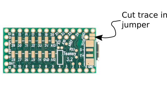
Since we're going to be powereing the Teensy from the regulator on the pedal circuit board, we want to cut the jumper that bridges the USB bus voltage to the Teensy power input. We used a hobby knife to cut the trace, and a continuity checker to make sure the cut was complete.
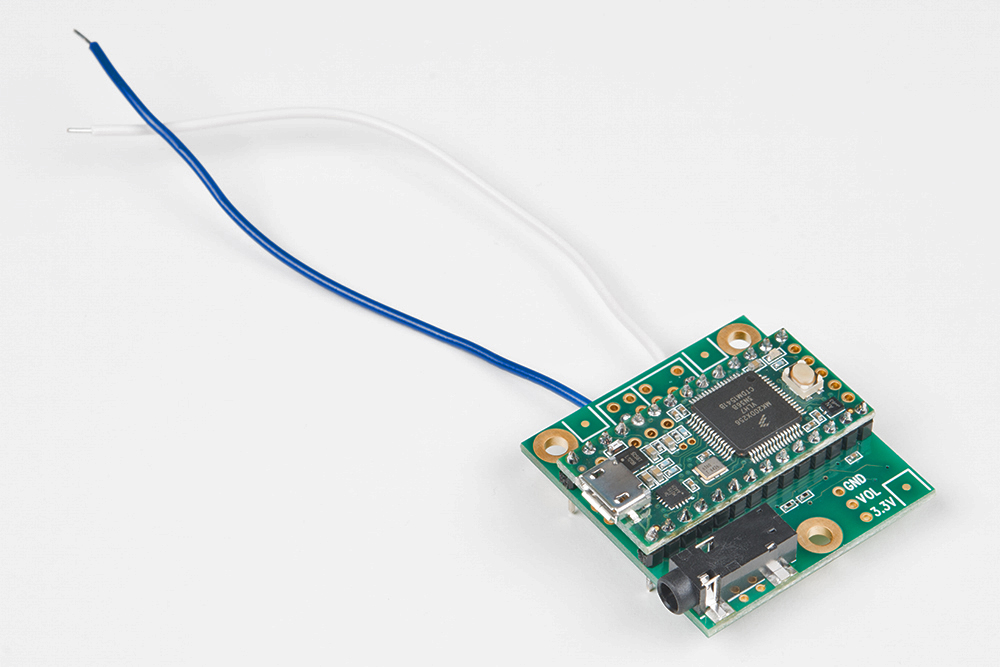
Next we want to stack the teensy and audio adapter with header pins.
The first step is to break off two 14-pin sections of snappable header, and solder them to the Teensy, with the longer portion of the pins pointing downwards. Below, we're using a small breadboard to hold the pins straight while we solder.
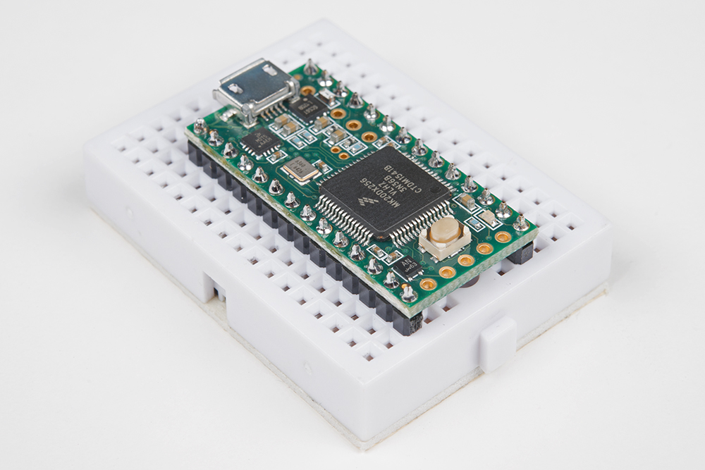
Then we remove the Teensy from the breadboard, and put the pins through the audio adapter. Double check the alignment before proceeding: the USB port on the Teensy and the headphone plug on the audio board both face the same direction.
The audio board gets soldered to the pins from below.
While we're looking at the bottom of the board, let's solder two more wires to the audio adapter. Here, you can see white and blue wires connected to the left line input and the left line output. Each wire is about 4 inches long -- we'll trim them to length later.
| Wire Color | Connection | Length |
|---|---|---|
| White | Line out L | 4 inches |
| Blue | Line In L | 4 inches |
They're inserted from the bottom of the board...
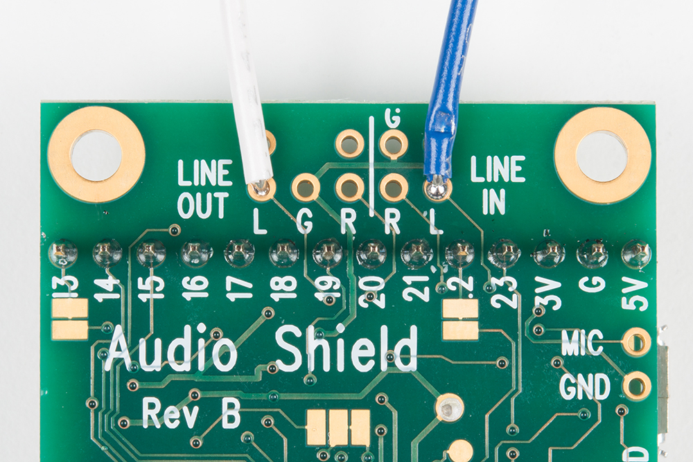
...and soldered to the top of the board.
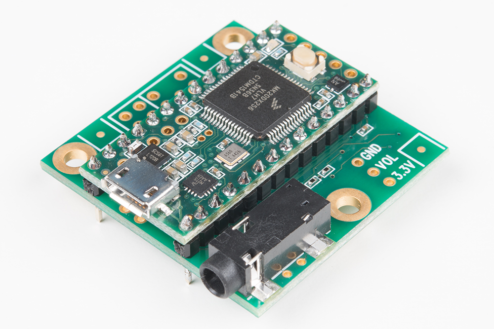
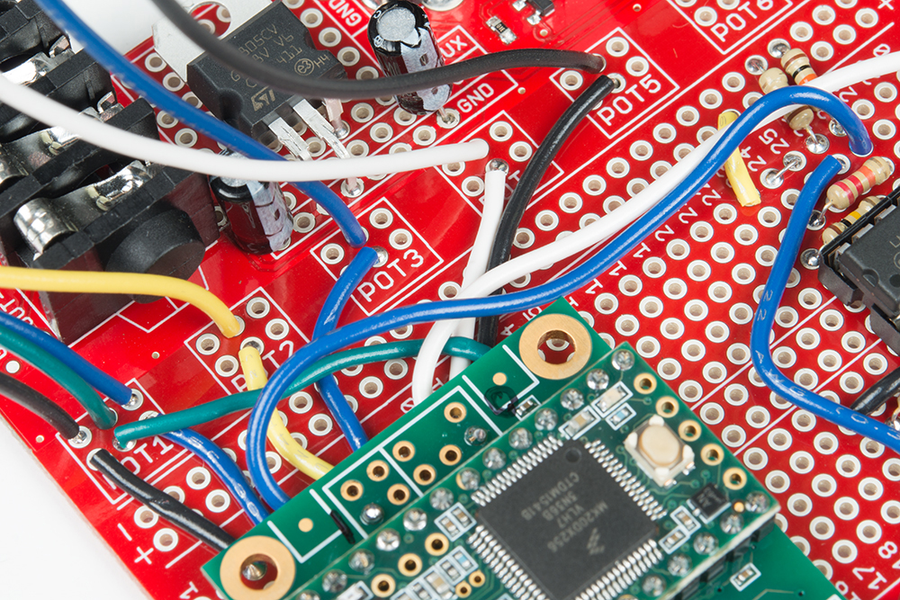
Now we put the stack on the proto pedal circuit board.

The stack is placed with the USB and headphone jacks pointing to the left, where the USB plug will align with the hole in the left side of the chassis. It spans from column 2 to column 15, and the pins were placed in rows C and G. We don't want to bottom of the audio adapter to accidentally touch anything on the pedal PCB, as we're using a coffee stirrer as a shim while we solder.
You can see the clearance between the stack and the pedal PCB below.
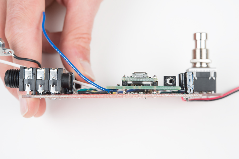
The last piece of this step is to run the wires from the line connections back to the analog section.
| Wire Color | Source | Destination |
|---|---|---|
| White | Line Out L | 25A |
| Blue | Line In L | 27I |
Before soldering, we ran the wires to their destination, and trimmed some excess, helping avoid clutter.
Incremental Test
Testing this step is similar to the previous incremental test. Connect the input, output and power. Then load the throughput sketch. This sketch allows the Teensy to pass audio from line input to line output.
Toggle the stomp switch a few times. The output of the pedal should be the same amplitude when it is engaged or bypassed. You will likely be able to hear the raised noise floor of the Teensy when the pedal is engaged.
Controls section
The final quadrant of the circuit is the panel controls. Like the previous step, we'll build a subassembly, then integrate it with the main circuit board.
To start, mount the five 10K potentiometers in the chassis, and tighten them in place. Notice that we've numbered each pot (1 through 5), and labeled it with it's corresponding Teensy ADC input (A12, A7, A6, A3 and A2). The numbers run right-to-left beacuse we're looking from the inside of the box.
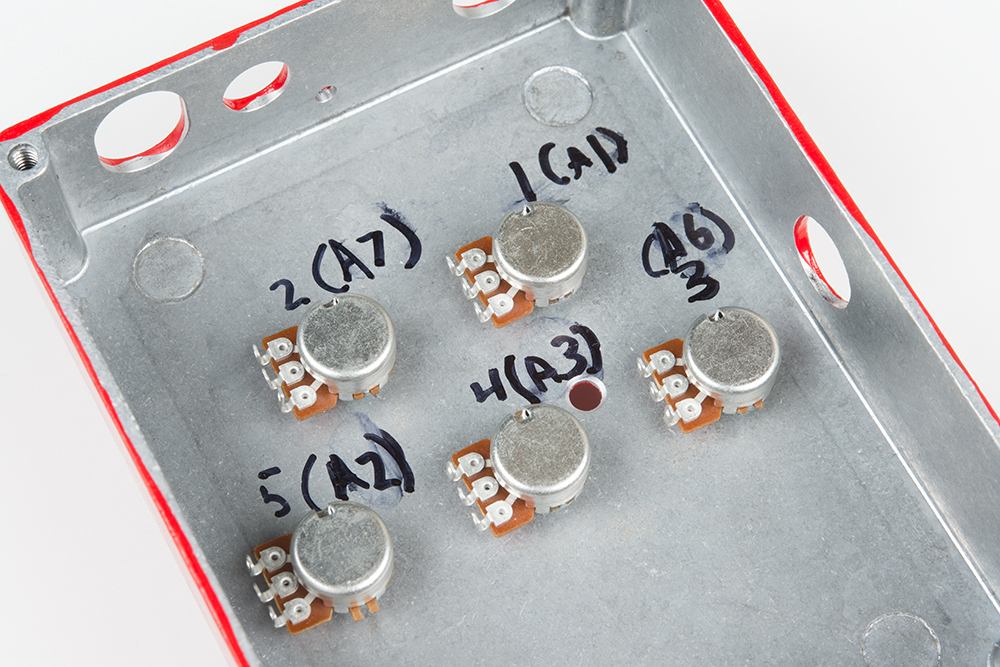
The pots are wired as parallel voltage dividers between the Teensy AGND and 3.3V signals. Since they're in parallel, they'll be wired as busses.

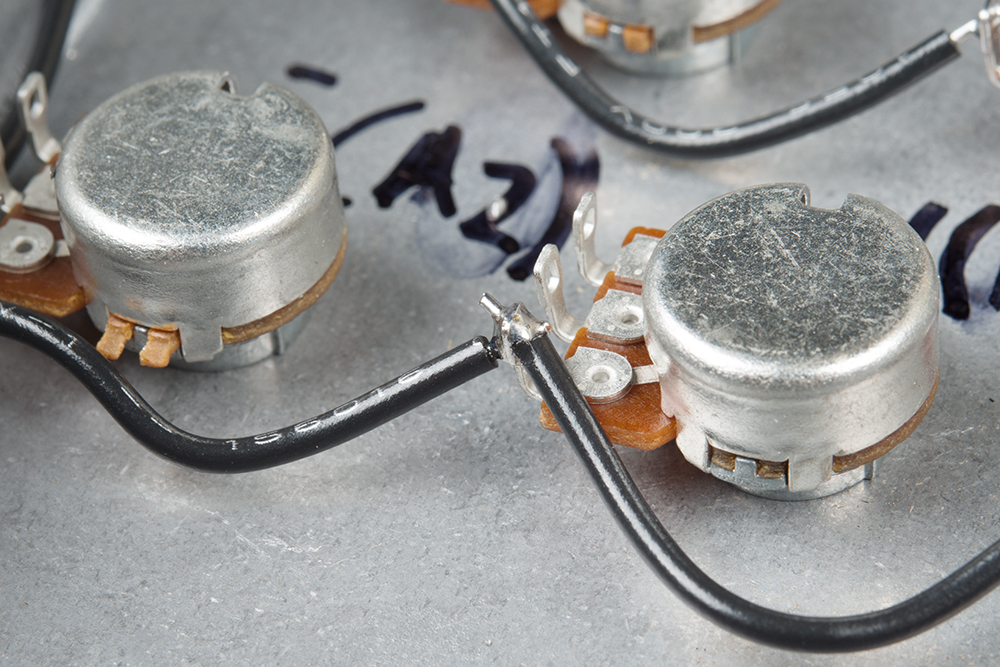
As indicated in the photo above, the left legs of the pots are daisy-chained with black wire, and the right legs are daisy-chained with blue wire. The middle terminal of each pot will get it's own color coded wire in a later step.
For the bus that runs from pot to pot, we used short pieces of solid core wire. Each leg in the daisy-chain has a wire to each of it's neighbors. We stripped the ends of each wire, then pushed them through the holes in the pot terminal.
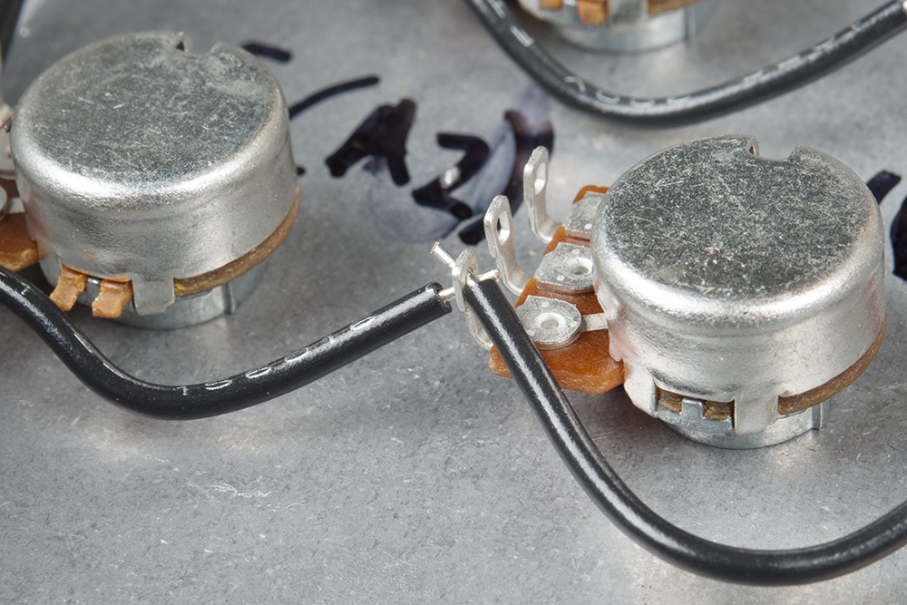
We then flow solder onto that nexus, making sure to avoid cold solder joints.
The black and blue daisy chains are run between pots, and then we add pigtails to run to the main PCB. Because these wires need to be flexible, we selected about 6 inches of stranded hookup wire, and soldered them to the end of the respective daisy chains.
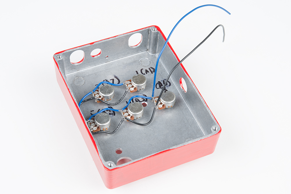
With the buses complete, we need to add five more wires to the potentiometer wipers. Again, we're using stranded hookup wire, each about 6 inches long.
The following table and photos illustrate the connections.
| Pot connection | Wire Color | Board Destination |
|---|---|---|
| Clockwise Bus | Blue | Pot1 Right |
| Counterclockwise Bus | Black | Pot1 Left |
| Wiper 1 | Green | Pot1 Middle |
| Wiper 2 | Yellow | Pot2 Middle |
| Wiper 3 | Blue | Pot3 Middle |
| Wiper 4 | White | Pot4 Middle |
| Wiper 5 | Black | Pot5 Middle |
When these wires in place, you should have wires as seen below. Note that we've got two blue and two black wires -- the wiper signals (to the left of the photo), and the daisy chained buses (to the right of the photo). Be careful to keep them straight when you connect them to the PCB!

The black and blue bus wires connect to the left and right pads of the Pot1 area, respectively. The blue wiper wire connects to the center of pot 3, and the black wiper wire connects to the center of pot 5.
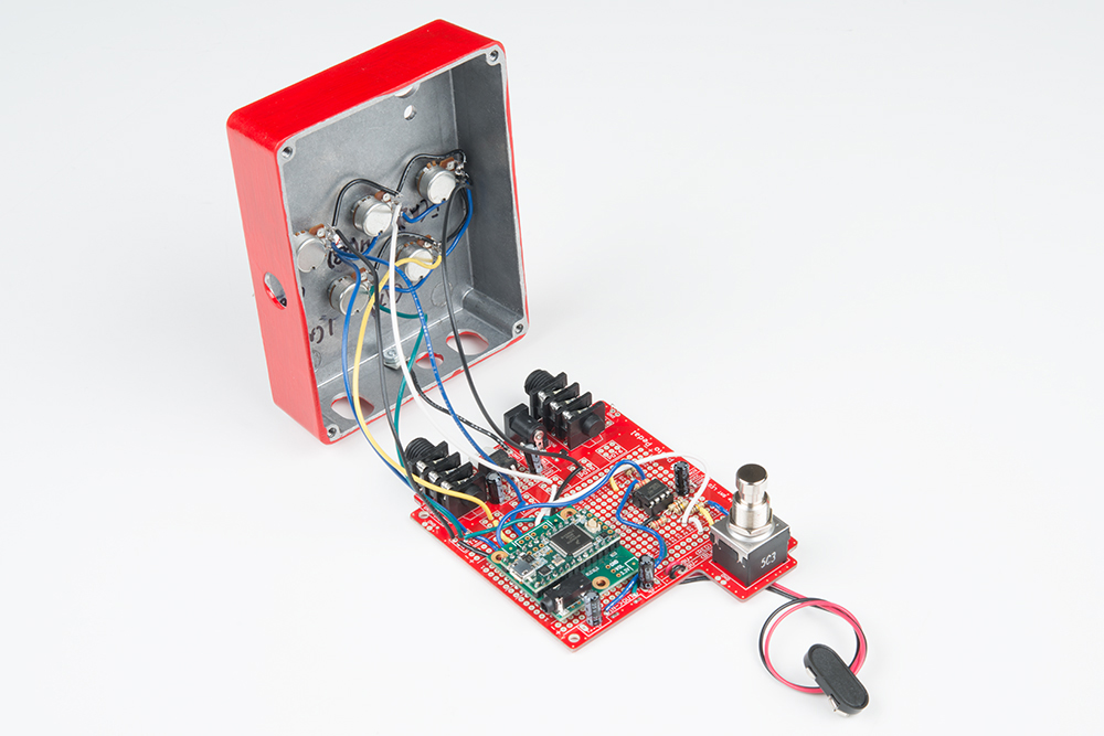
With the controls soldered to the PCB, you should have an overall assembly as depicted below.
Notice that we've also bolted the ground lug from the PCB to the chassis.
Final Incremental Test
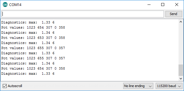
The throughput test sketch that we loaded in the last step also serves as an integration test for the panel controls. If you open the serial port, you notice that it periodically prints a set of five values, showing the potentiometer readings. As you turn each pot, the values should change from 0 when set counterclockwise, to 1023 at when fully clockwise.
Close It Up
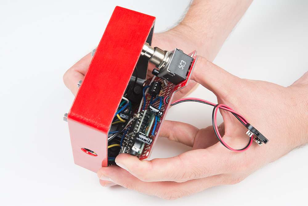
When the tests are passing, we're done soldering, and we can close the pedal up.
To put the PCB into the chassis, angle it so the TRS jacks go through the oblong holes, then pivot the board so the switch goes through its hole. As it closes, make sure that the control wires aren't hanging up on anything, and if you've got a PTH LED, take care to get it through the chassis hole, too.
Then put the external hardware on to hold the board in place. The switch gets a hex nut, and each TRS jack has a plastic washer and hex nut.
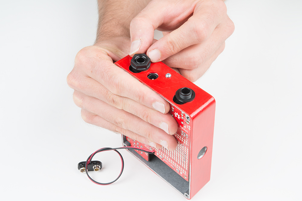
Before you tighten all of the hardware, doublecheck the aliignment of the barrel jack. It should be centered in the panel hole, as shown below. This alignment reduces the chances of the barrel jack shorting to the chassis, or the bottom of the PCB coming into contact with the lid of the enclosure.
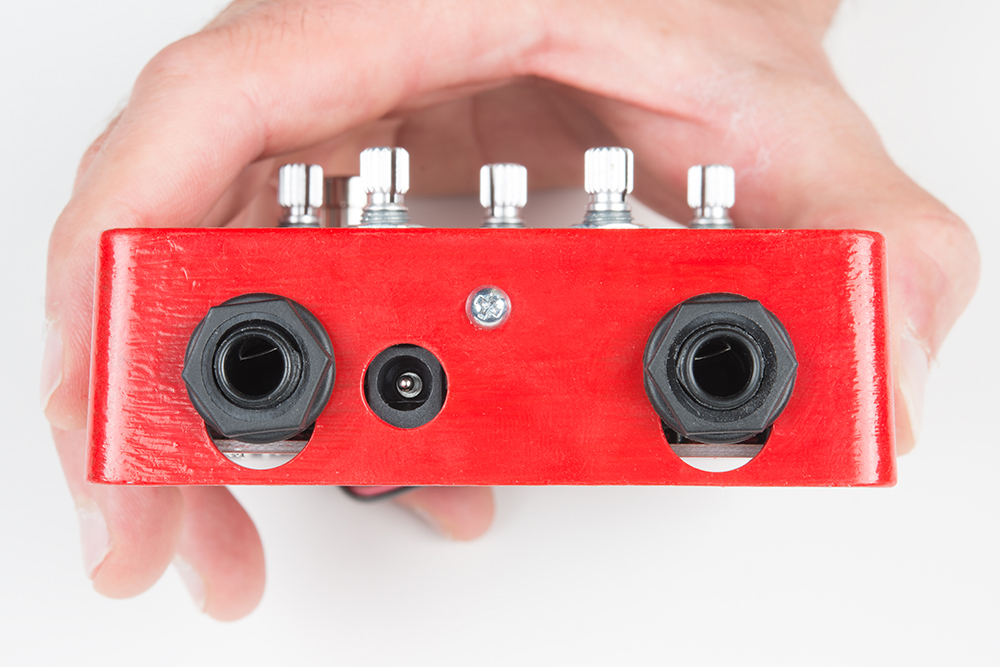
Finally, put the back on the box, and put knobs on the pots.
Add the Software
It's up to your imagination to come up with the effect you want, but here's a few you can load right in and try.
They can be found in the teensy sketches directory in the Proto Pedal github repository.
Throughput
We've already used the throughput sketch to test the audio hardware. It simply passes audio straight from the input to the output. Boring, but you can use it to make sure your system is working!
You can also use this as a template when creating new sketches.
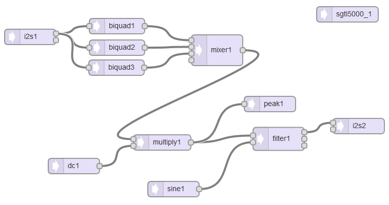
AutoRoller
The AutoRoller has an input filter for tone control, an output low-pass filter for effect, and a modulation source consisting of a sine wave generator with rate dependent on input peak values. The louder you play, the faster the filter sweeps. It creates a dynamically controlled warble, similar to a rotary tone cabinet.
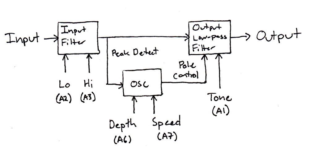
Within the AutoRoller patch, the input hits a tone control, which allows the relative tonal balance to be adjusted. From there, it feeds a peak detector module. The output of the peak detector modulates the frequency of a sine wave, which is used to modulate the lowpass filter. The 'tone' knob is used to set the nominal characteristics of the output filter, combining cutoff frequency and resonance on a single knob.
More information about the AutoRoller can be found in the readme and other files in the repository.
Tape Echo Emulation
Finally, we've got an example of a tape echo emulation.
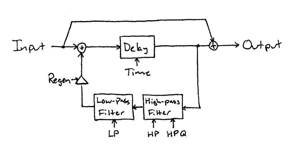
It consists of a delay line with highpass and lowpass filters in the feedback loop. It can be used as a subtly colored digital delay, or tweaked into an interactive, regenerative sound effect generator.
You can find the sketch and related files here.
Please note: the README.md file for the echo contains some additional information about compiling the effect. In order to have the maximum amount of RAM available for the delay line, be sure to select a non-optimized build configuration in the tools->cpu speed menu.
Resources and Going Further
Resources
- The Proto Pedal Assembly and Theory guide.
- The chassis hookup guide.
- The Teeny Audio Homepage has more background on Teensy audio.
- Some of our digital effects have been influenced by designs from MusicDSP.org.
- Hal Chamberlin's long out-of-print Musical Applications of Microprocessors has also proven to be a valuable reference, and an intuitive entry point to the math-heavy world of digital signal processing.
Going Further
This guide is really just the starting point - what you ultimately create depends on your imagination, and how clever you are at using the Teensy Audio library!