Multiplexer Breakout Hookup Guide
 jimblom
74HC4051 Breakout Overview
The Multiplexer Breakout's schematic is just about as simple as it gets: There's the chip, a decoupling capacitor, a pull-up resistor, and all of the pins are broken out (some broken out twice):
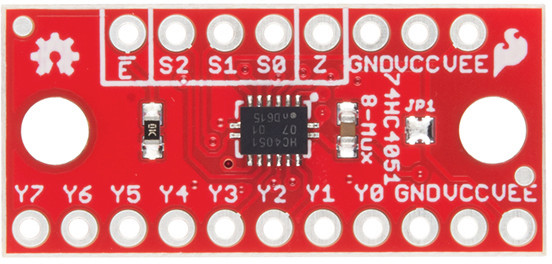
One half of the board breaks out the control signals (E, S0-S2) and common input/output (Z). The other side provides access to all eight independent I/O's (Y0-Y7). Both sides include supply and ground connections (VCC, VEE, GND). The table below summarizes each pin and its function.
| Pin Label | Function | Input/Output (to board) | Notes |
|---|---|---|---|
| E | Enable | Input | Active low enable |
| S2, S1, S0 | Select Controls | Input | Select inputs, S2 is the msb and S0 is the lsb |
| Z | Common I/O | Input/Output | Common output or input |
| GND | Ground | Supply | Ground supply voltage (0V) |
| VCC | Positive supply | Supply | Positive supply voltage (2-10V) |
| VEE | Negative supply | Supply | Negative supply voltage (Jumpered to ground by default) |
| Y7, Y6, Y5, Y4, Y3, Y2, Y1, Y0 | Independent I/O | Input/Output | Selectable I/O to be routed to common pin |
74HC4051 Logic Table
The select pins (S2-S0), in addition to the enable pin (E), control which (if any) of the eight independent I/O pins (Y0-Y7) are connected to the common pin (Z). The function table below shows how those pins work together to select the I/O.
| E | S2 | S1 | S0 | I/O Connected to Z |
|---|---|---|---|---|
| L | L | L | L | Y0 |
| L | L | L | H | Y1 |
| L | L | H | L | Y2 |
| L | L | H | H | Y3 |
| L | H | L | L | Y4 |
| L | H | L | H | Y5 |
| L | H | H | L | Y6 |
| L | H | H | H | Y7 |
| H | X | X | X | None |
Assuming the mux is powered at 5V, "L," for "low", is any voltage between 0 and about 2V and "H" -- "high" -- is any voltage between around 3 and 5V. "X" means it doesn't matter what the logic level of the pin is (because it will be trumped by the enable pin).
Power Supply Limits
The 74HC4051 supports a wide supply range, but the presence of the optional negative voltage supply -- VEE -- has the potential to make things a little complicated. Here are the basic rules that govern the 74HC4051's power supplies:
- VCC must be at least 2.0V (above GND).
- VCC must not exceed 10V (above GND).
- VEE must be less than VCC -- anywhere between 2.0V and 10V below VCC.
The operating area graph below -- figure 7 in the datasheet -- represents those ranges visually:

For example, the 74HC4051 supports standard 3.3V, 5V, and 9V supplies, as well as bipolar supplies, like ±5V (but not ±9V).
JP1 -- Connecting VEE to GND
We expect that the majority of multiplexer-equipped projects may not need the 74HC4051's bipolar supply support. So, to make the board easier to get quickly up-and-running, we've added a jumper to the top side, which shorts VEE to GND.
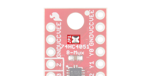
By connecting VEE to GND, you can satisfy both VCC-GND and VCC-VEE limits by keeping VCC between 2.0 and 10.0V. Unless you need a bipolar supply, you can leave this jumper closed and ignore VEE entirely.
Using a Bipolar Power Supply
The 74HC4051 supports bi-polar power supplies, with a positive supply on VCC and a negative supply on VEE. The difference between VCC and VEE can be as much as 10V (e.g. ±5V), but VCC must be somewhere between 2V and 10V.
To use a bipolar supply, you must first open JP1, disconnecting VEE from GND.

A quick hit of a soldering iron on some solder wick should lift that solder right up.
Once the jumper is open, your supplies can be connected. The logic levels of the select and enable pins will still be limited by VCC, but your common pin and eight I/O pins will be able to range between VEE and VCC.