MicroMod STM32 Processor Hookup Guide
 Alex the Giant, Ell C
Hardware Overview
M.2 Connector
All of our MicroMod Processor boards come equipped with the M.2 MicroMod Connector, which leverages the M.2 standard and specification to allow you to install your MicroMod Processor board on your choice of carrier board.
 |
 |
| M.2 Connector from the Front | M.2 Connector from the Back |
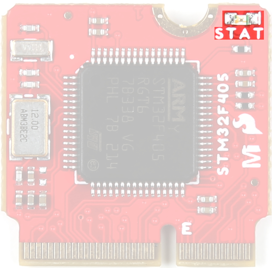
STM32F405
There is so much packed into this chip! As stated in the introduction, STMicroelectronics' STM32F405RG family is based on the ARM Cortex M4 RISC core. At 168MHz, it provides very high performance, floating point single precision, a full set of DSP instructions, and a memory protection unit that enhances application security. For more information, refer to the Datasheet.

Power
Power is supplied by the carrier board, but it should be noted that all pins are 3.3V.
Boot and Reset Buttons
In order to upload code to the STM32 MicroMod Processor Board, you'll need these two buttons to put the board into Boot mode. Hold the Boot button down, press the Reset button (while still holding the Boot button), and then release the Boot button.
These pins will be on the carrier board. For this tutorial, we will show you the these pins on the MicroMod ATP Carrier board.

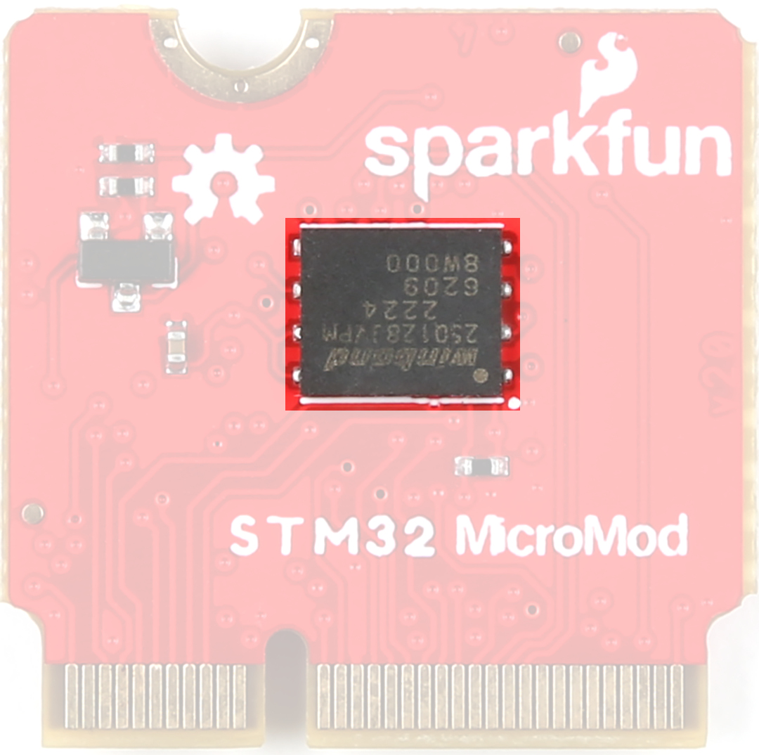
Flash
To complement the STM32F405 processor, we've added an additional 128Mb (16MB) serial flash memory chip.
Status LED
MicroMod STM32F405 Processor Pin Functionality
The complete pin map can be found in the table below or you can refer to the schematic.
| AUDIO | UART | GPIO/BUS | I2C | SDIO | SPI | Dedicated |
| STM32 Pin | Primary Function | Bottom Pin |
Top Pin |
Primary Function | STM32 Pin |
|---|---|---|---|---|---|
| - | (Not Connected) | 75 | GND | - | |
| - | 3.3V | 74 | 73 | G5 / BUS5 | PC13 |
| - | - | 72 | 71 | G6 / BUS6 | PC2 |
| - | - | 70 | 69 | - | - |
| - | - | 68 | 67 | - | - |
| - | - | 66 | 65 | - | - |
| - | - | 64 | 63 | G10/HOST_VBUS | PB13 |
| - | - | 62 | 61 | SPI_PICO (I) | PA6 |
| - | - | 60 | 59 | SPI_POCI (O) | PA7 |
| - | - | 58 | 57 | SPI_SCK (O) | PA5 |
| PB4 | AUD_OUT | 56 | 55 | SPI_CS# | PC4 |
| PB5 | AUD_IN | 54 | 53 | I2C_SCL1 (I/O) | PB6 |
| PA4 | AUD_LRCLK | 52 | 51 | I2C_SDA1 (I/O) | PB7 |
| PB3 | AUD_BCLK | 50 | 49 | BATT_VIN / 3 (I - ADC) (0 to 3.3V) | - |
| PC9 | G4 / BUS4 | 48 | 47 | PWM1 | PC7 |
| PC8 | G3 / BUS3 | 46 | 45 | GND | - |
| PA0 | G2 / BUS2 | 44 | 43 | CAN_TX | PB9 |
| PA8 | G1 / BUS1 | 42 | 41 | CAN_RX | PB8 |
| PD2 | G0 / BUS0 | 40 | 39 | GND | - |
| PB0 | A1 | 38 | 37 | USBHOST_D- | PB14 |
| - | GND | 36 | 35 | USBHOST_D+ | PB15 |
| PC5 | A0 | 34 | 33 | GND | - |
| PC6 | PWM0 | 32 | 31 | Module Key | - |
| - | Module Key | 30 | 29 | Module Key | - |
| - | Module Key | 28 | 27 | Module Key | - |
| - | Module Key | 26 | 25 | Module Key | - |
| - | Module Key | 24 | 23 | SWDIO | PA13 |
| - | - | 22 | 21 | SWCLK | PA14 |
| - | - | 20 | 19 | UART_RX1 (I) | PA10 |
| PC1 | D1 | 18 | 17 | UART_TX1 (0) | PA9 |
| PB1 | I2C_INT# | 16 | 15 | - | - |
| PB10 | I2C_SCL (I/0) | 14 | 13 | - | - |
| PB11 | I2C_SDA (I/0) | 12 | 11 | BOOT# (I - Open Drain) | BOOT0 |
| PC0 | D0 | 10 | 9 | - | - |
| PB12 | G11/HOST_ID | 8 | 7 | GND | - |
| - | RESET# (I - Open Drain) | 6 | 5 | USB_D- | PA11 |
| - | - | 4 | 3 | USB_D+ | PA12 |
| - | 3.3V | 2 | 1 | GND | - |
| Function | Bottom Pin |
Top Pin |
Function | ||||||
|---|---|---|---|---|---|---|---|---|---|
| (Not Connected) | 75 | GND | |||||||
| 3.3V | 74 | 73 | G5 / BUS5 | ||||||
| RTC_3V_BATT | 72 | 71 | G6 / BUS6 | ||||||
| SPI_CS1# | SDIO_DATA3 (I/O) | 70 | 69 | G7 / BUS7 | |||||
| SDIO_DATA2 (I/O) | 68 | 67 | G8 | ||||||
| SDIO_DATA1 (I/O) | 66 | 65 | G9 | ADC_D- | CAM_HSYNC | ||||
| SPI_PICO1 | SDIO_DATA0 (I/O) | 64 | 63 | G10 | ADC_D+ | CAM_VSYNC | |||
| SPI POCI1 | SDIO_CMD (I/O) | 62 | 61 | SPI_PICO (I) | |||||
| SPI SCK1 | SDIO_SCK (O) | 60 | 59 | SPI_POCI (O) | LED_DAT | ||||
| AUD_MCLK (O) | 58 | 57 | SPI_SCK (O) | LED_CLK | |||||
| CAM_MCLK | PCM_OUT | I2S_OUT | AUD_OUT | 56 | 55 | SPI_CS# | |||
| CAM_PCLK | PCM_IN | I2S_IN | AUD_IN | 54 | 53 | I2C_SCL1 (I/O) | |||
| PDM_DATA | PCM_SYNC | I2S_WS | AUD_LRCLK | 52 | 51 | I2C_SDA1 (I/O) | |||
| PDM_CLK | PCM_CLK | I2S_SCK | AUD_BCLK | 50 | 49 | BATT_VIN / 3 (I - ADC) (0 to 3.3V) | |||
| G4 / BUS4 | 48 | 47 | PWM1 | ||||||
| G3 / BUS3 | 46 | 45 | GND | ||||||
| G2 / BUS2 | 44 | 43 | CAN_TX | ||||||
| G1 / BUS1 | 42 | 41 | CAN_RX | ||||||
| G0 / BUS0 | 40 | 39 | GND | ||||||
| A1 | 38 | 37 | USBHOST_D- | ||||||
| GND | 36 | 35 | USBHOST_D+ | ||||||
| A0 | 34 | 33 | GND | ||||||
| PWM0 | 32 | 31 | Module Key | ||||||
| Module Key | 30 | 29 | Module Key | ||||||
| Module Key | 28 | 27 | Module Key | ||||||
| Module Key | 26 | 25 | Module Key | ||||||
| Module Key | 24 | 23 | SWDIO | ||||||
| UART_TX2 (O) | 22 | 21 | SWDCK | ||||||
| UART_RX2 (I) | 20 | 19 | UART_RX1 (I) | ||||||
| CAM_TRIG | D1 | 18 | 17 | UART_TX1 (0) | |||||
| I2C_INT# | 16 | 15 | UART_CTS1 (I) | ||||||
| I2C_SCL (I/0) | 14 | 13 | UART_RTS1 (O) | ||||||
| I2C_SDA (I/0) | 12 | 11 | BOOT (I - Open Drain) | ||||||
| D0 | 10 | 9 | USB_VIN | ||||||
| SWO | G11 | 8 | 7 | GND | |||||
| RESET# (I - Open Drain) | 6 | 5 | USB_D- | ||||||
| 3.3V_EN | 4 | 3 | USB_D+ | ||||||
| 3.3V | 2 | 1 | GND | ||||||
| Signal Group | Signal | I/O | Description | Voltage | Power | 3.3V | I | 3.3V Source | 3.3V |
|---|---|---|---|---|
| GND | Return current path | 0V | ||
| USB_VIN | I | USB VIN compliant to USB 2.0 specification. Connect to pins on processor board that require 5V for USB functionality | 4.8-5.2V | |
| RTC_3V_BATT | I | 3V provided by external coin cell or mini battery. Max draw=100μA. Connect to pins maintaining an RTC during power loss. Can be left NC. | 3V | |
| 3.3V_EN | O | Controls the carrier board's main voltage regulator. Voltage above 1V will enable 3.3V power path. | 3.3V | |
| BATT_VIN/3 | I | Carrier board raw voltage over 3. 1/3 resistor divider is implemented on carrier board. Amplify the analog signal as needed for full 0-3.3V range | 3.3V | |
| Reset | Reset | I | Input to processor. Open drain with pullup on processor board. Pulling low resets processor. | 3.3V |
| Boot | I | Input to processor. Open drain with pullup on processor board. Pulling low puts processor into special boot mode. Can be left NC. | 3.3V | |
| USB | USB_D± | I/O | USB Data ±. Differential serial data interface compliant to USB 2.0 specification. If UART is required for programming, USB± must be routed to a USB-to-serial conversion IC on the processor board. | |
| USB Host | USBHOST_D± | I/O | For processors that support USB Host Mode. USB Data±. Differential serial data interface compliant to USB 2.0 specification. Can be left NC. | |
| CAN | CAN_RX | I | CAN Bus receive data. | 3.3V |
| CAN_TX | O | CAN Bus transmit data. | 3.3V | |
| UART | UART_RX1 | I | UART receive data. | 3.3V |
| UART_TX1 | O | UART transmit data. | 3.3V | |
| UART_RTS1 | O | UART ready to send. | 3.3V | |
| UART_CTS1 | I | UART clear to send. | 3.3V | |
| UART_RX2 | I | 2nd UART receive data. | 3.3V | |
| UART_TX2 | O | 2nd UART transmit data. | 3.3V | |
| I2C | I2C_SCL | I/O | I2C clock. Open drain with pullup on carrier board. | 3.3V |
| I2C_SDA | I/O | I2C data. Open drain with pullup on carrier board | 3.3V | |
| I2C_INT# | I | Interrupt notification from carrier board to processor. Open drain with pullup on carrier board. Active LOW | 3.3V | |
| I2C_SCL1 | I/O | 2nd I2C clock. Open drain with pullup on carrier board. | 3.3V | |
| I2C_SDA1 | I/O | 2nd I2C data. Open drain with pullup on carrier board. | 3.3V | |
| SPI | SPI_POCI | O | SPI Controller Output/Peripheral Input. | 3.3V |
| SPI_PICO | I | SPI Controller Input/Peripheral Output. | 3.3V | |
| SPI_SCK | O | SPI Clock. | 3.3V | |
| SPI_CS# | O | SPI Chip Select. Active LOW. Can be routed to GPIO if hardware CS is unused. | 3.3V | |
| SPI/SDIO | SPI_SCK1/SDIO_CLK | O | 2nd SPI Clock. Secondary use is SDIO Clock. | 3.3V |
| SPI_POCI1/SDIO_CMD | I/O | 2nd SPI Controller Output/Peripheral Input. Secondary use is SDIO command interface. | 3.3V | |
| SPI_PICO1/SDIO_DATA0 | I/O | 2nd SPI Peripheral Input/Controller Output. Secondary use is SDIO data exchange bit 0. | 3.3V | |
| SDIO_DATA1 | I/O | SDIO data exchange bit 1. | 3.3V | |
| SDIO_DATA2 | I/O | SDIO data exchange bit 2. | 3.3V | |
| SPI_CS1/SDIO_DATA3 | I/O | 2nd SPI Chip Select. Secondary use is SDIO data exchange bit 3. | 3.3V | |
| Audio | AUD_MCLK | O | Audio master clock. | 3.3V |
| AUD_OUT/PCM_OUT/I2S_OUT/CAM_MCLK | O | Audio data output. PCM synchronous data output. I2S serial data out. Camera master clock. | 3.3V | |
| AUD_IN/PCM_IN/I2S_IN/CAM_PCLK | I | Audio data input. PCM syncrhonous data input. I2S serial data in. Camera periphperal clock. | 3.3V | |
| AUD_LRCLK/PCM_SYNC/I2S_WS/PDM_DATA | I/O | Audio left/right clock. PCM syncrhonous data SYNC. I2S word select. PDM data. | 3.3V | |
| AUD_BCLK/PCM_CLK/I2S_CLK/PDM_CLK | O | Audio bit clock. PCM clock. I2S continuous serial clock. PDM clock. | 3.3V | |
| SWD | SWDIO | I/O | Serial Wire Debug I/O. Connect if processor board supports SWD. Can be left NC. | 3.3V |
| SWDCK | I | Serial Wire Debug clock. Connect if processor board supports SWD. Can be left NC. | 3.3V | |
| ADC | A0 | I | Analog to digital converter 0. Amplify the analog signal as needed to enable full 0-3.3V range. | 3.3V |
| A1 | I | Analog to digital converter 1. Amplify the analog signal as needed to enable full 0-3.3V range. | 3.3V | |
| PWM | PWM0 | O | Pulse width modulated output 0. | 3.3V |
| PWM1 | O | Pulse width modulated output 1. | 3.3V | |
| Digital | D0 | I/O | General digital input/output pin. | 3.3V |
| D1/CAM_TRIG | I/O | General digital input/output pin. Camera trigger. | 3.3V | |
| General/Bus | G0/BUS0 | I/O | General purpose pins. Any unused processor pins should be assigned to Gx with ADC + PWM capable pins given priority (0, 1, 2, etc.) positions. The intent is to guarantee PWM, ADC and Digital Pin functionality on respective ADC/PWM/Digital pins. Gx pins do not guarantee ADC/PWM function. Alternative use is pins can support a fast read/write 8-bit or 4-bit wide bus. | 3.3V |
| G1/BUS1 | I/O | 3.3V | ||
| G2/BUS2 | I/O | 3.3V | ||
| G3/BUS3 | I/O | 3.3V | ||
| G4/BUS4 | I/O | 3.3V | ||
| G5/BUS5 | I/O | 3.3V | ||
| G6/BUS6 | I/O | 3.3V | ||
| G7/BUS7 | I/O | 3.3V | ||
| G8 | I/O | General purpose pin | 3.3V | |
| G9/ADC_D-/CAM_HSYNC | I/O | Differential ADC input if available. Camera horizontal sync. | 3.3V | |
| G10/ADC_D+/CAM_VSYNC | I/O | Differential ADC input if available. Camera vertical sync. | 3.3V | |
| G11/SWO | I/O | General purpose pin. Serial Wire Output | 3.3V |
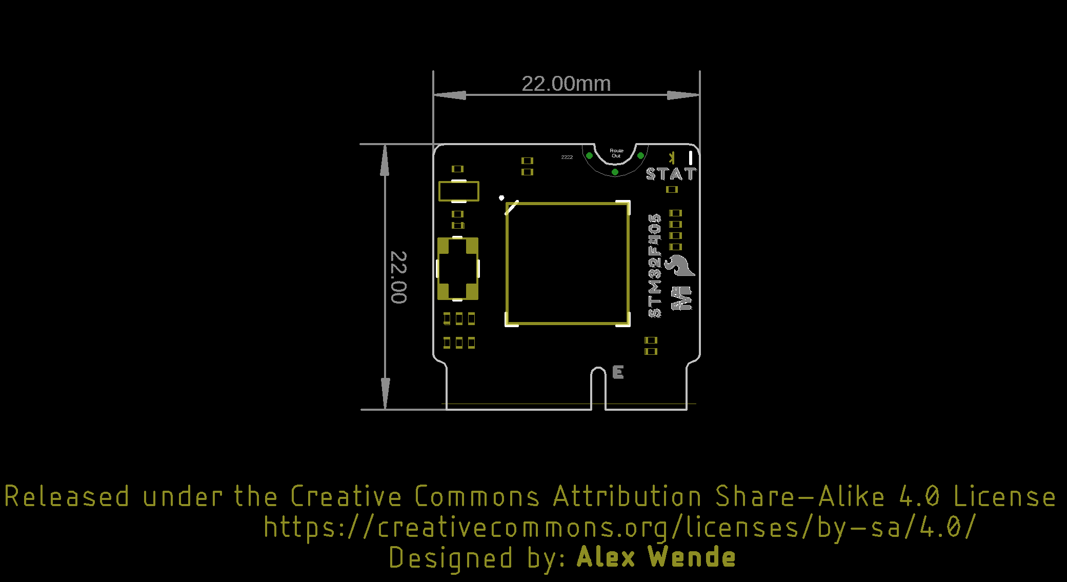
Board Outline
The board takes advantage of the standard MicroMod form factor.