FreeSoC2 Introduction
This Tutorial is Retired!
Note: This guide is for the previous version of the FreeSoC2, V11. If you have an newer version (the version number can be found on the back of the PCB), please refer to this tutorial.
View the updated tutorial: FreeSoC2 Hookup Guide V14
Contributors:
 SFUptownMaker
SFUptownMaker 
Hardware Overview
There's a lot going on on this board: two processors, two USB ports, a ton of headers, and all sorts of configurable options.
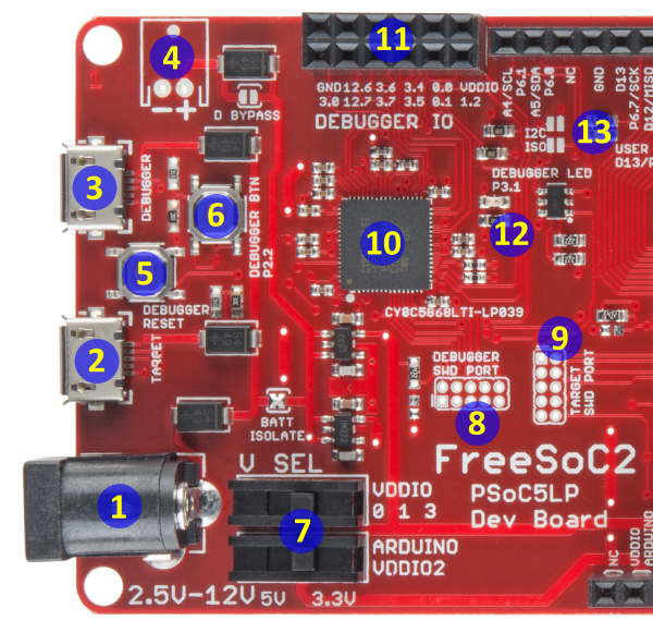
We'll take a hardware tour, one element at a time, starting with the debugging and connection elements on the left.
- 5.5mm x 2.1mm center positive barrel jack--This fits all of SparkFun's standard "wall wart" type power supplies. While the regulators on the FreeSoC2 can handle input voltages up to 12V, it's best to keep the input voltage as close to 5V as possible.
- "Target" USB Port--Provides USB connectivity to the target processor (the CY8C5888). When uploading code via the Arduino IDE, you'll connect to this port.
- "Debugger" USB Port--Connects to the debugger IC. Connecting to this port also creates a USB serial port which can be used to get and send data from and to a UART on the target processor.
- 2.5mm JST PH series connector footprint--Our through hole 2-pin JST PH connector fits here, allowing you to power the board with any of our standard lithium ion polymer batteries.
- Debugger reset button--Resets the debugger. You will probably never need to use this.
- Debugger user button--Can be used to provide input to the debugger IC; currently unused.
- IO voltage selection switches--These switches allow you to select the voltage of the I/O signals, either 3.3V or 5V, on the target processor. The PSoC5LP has four I/O voltage quadrants; the bottom switch allows you to select the voltage of the quadrant providing the Arduino header signals and the top switch, all the others.
- Debugger IC JTAG/SWD header--This 2x5 0.050" pitch header can be used to program and debug the debugger itself. It's intended to support a connection to the MiniProg3 programmer/debugger from Cypress. You'll probably never need to use it.
- Target IC JTAG/SWD header--Similar in nature to the header for the debugger; the signals on these pins also come from the debugger IC.
- Debugger IC--The debug IC is also a PSoC5LP- in this case, CY8C5868LTI-LP039. The firmware it comes preloaded with (referred to as "KitProg") is freely available for download and modification; the part is bootloadable to replace the firmware or update it as new firmware becomes available.
- Debugger IC IO header--There are a number of signals available on this header; they are not used by default but you may implement additional debugging features on the debugger IC that do use them.
- Debugger IC user LED--Will be lit if the debugger can't detect a host, and will flash during data transfer (i.e., programming or debugging).
- I2C isolation jumpers--These normally open solder jumpers allow you to connect the I2C lines on the target board with the debugger. Using Cypress's KitProg debugging software, you can snoop the I2C data traffic from the target IC. Normally, these are open, disabling this capability. Close them with solder blobs to connect the debugger to the target's I2C bus.
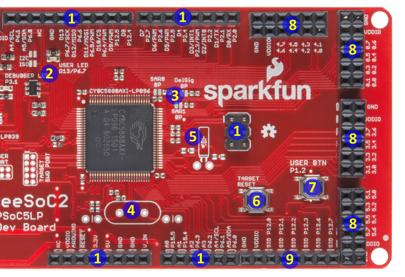
The right half of the board contains the target IC (a CY8C5888AXI-LP096) and the associated headers.
- Arduino Uno R3-type headers--For the most part, these headers are completely compatible with the Uno R3 board. The only exception is the VREF pin, normally located between the I2C pins and the ground above D13, is no-connect for this board.
- Target user LED--Tied to port 6, pin 7, which corresponds to D13 on the Arduino mapped headers.
- ADC reference bypass capacitor jumpers--These jumpers allow you to add a 100nF capacitor to three of the PSoC part's pins, to provide a bypass for ADC voltage references to increase the reference's accuracy.
- High-frequency crystal footprint--if you need better accuracy than can be achieved by the onboard oscillator, you may add a standard HC/49 crystal here.
- Low-frequency crystal fooprint--if you want to implement an RTC, you may add a 32.768kHz clock crystal here.
- Target IC reset button--This button resets only the target IC.
- Target IC user button--This button can be mapped to any purpose within the application; the button pulls down to ground and is not tied to any other header.
- Additional IO headers--These 2x6 headers are all additional I/O, and their voltage level (along with the voltage present on the VDDIO pins of those headers) is controlled by the top VDDIO set switch on the left end of the board and can be set to either 3.3V or 5V.
- SIO pins--These six pins are special, in that they can be connected to a signal voltage which is higher than their nominal I/O voltage. They can, of course, be used normally as well. This allows these pins to be 5V tolerant when the rest of the IO pins are running at 3.3V.