Designing with MicroMod
 Nate
Nate 
How to Design a MicroMod Processor Board
Instead of starting from scratch, we'll start with a known good development board. In this case, we'll start with a development board and convert it to a MicroMod Processor Board (PB).
Schematic
Start with a known good development board product, the SAMD51 Thing Plus for example, and remove all the bits from the EAGLE design that are not needed from the schematic:
- USB connector
- Qwiic connector
- JST connector
- Standoffs
- Headers
- Power regulation
- Reset buttons
- Silk
- TX/RX LEDs
- Battery charging
Keep any needed external circuitry such as:
- Decoupling
- ADC amplification
- Crystals for main clock of RTC
- External memory to enable Python script loading
- 1 status LED (usually connected to LED_BUILTIN)
- USB to serial conversion IC and circuitry
Keep anything needed for the device to be programmed by only USB +/-. This means you may need to include a USB to serial IC (CH340E is recommended) for devices that don’t have built-in USB peripherals. Retain any boot control circuitry (Artemis and ESP32 have boot pins that need to be controlled by RTS/DTR).
Remove all LED indicators that will be relocated to the carrier board. This includes TX/RX LEDs, Power LEDs, charge LEDs, etc. The exception to this is every Processor Board shall include one status LED connected to a pin that is not connected to the board edge. This enables the user to immediately test their processor board agnostic of the capabilities of the carrier board.
Check to see if there have been any changes or improvements to the general design using this processor. For a hypothetical example, users may be populating the SAMD51 boards with a 32mbit flash as opposed to the older 16mbit flash. Roll these improvements into the design.
Now is your chance to clean up the schematic component for the processor. Combine duplicate GND pins, VDDIO pins, etc into single pins on the schematic component.
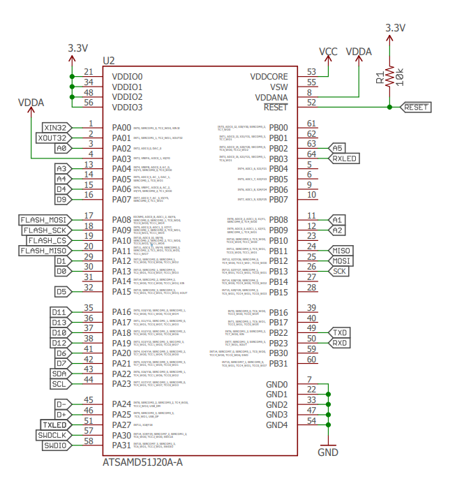
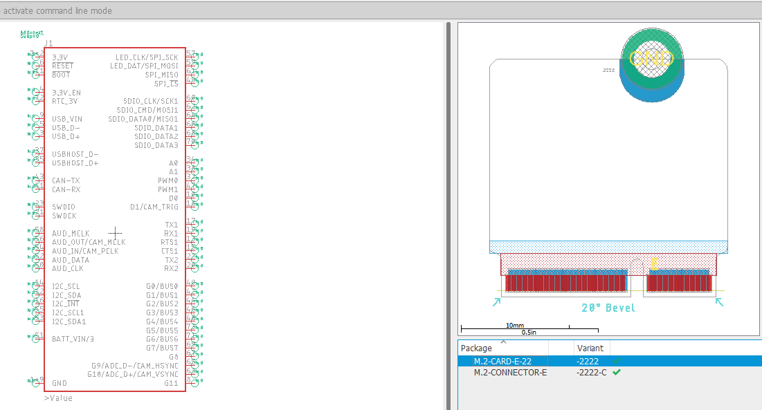
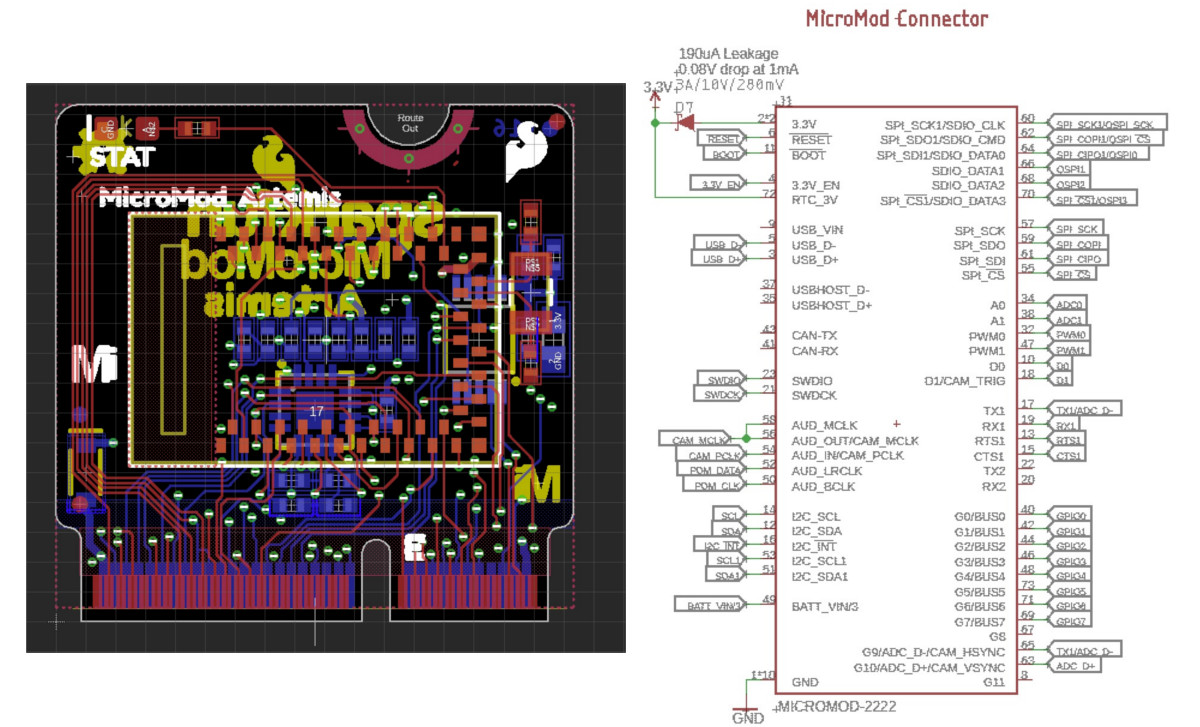
Pull in the MicroMod card edge connector from the SparkFun Eagle library. You'll find it under 'SparkFun-MicroMod'.
In the schematic, begin connecting the various dedicated hardware pins on the microcontroller to the MM card edge. For example, on the SAMD51:
- Connect USB +/- on processor to USB +/- on MM edge connector
- Primary I2C pins on SAMD51 connect to primary I2C pins on MM
- Flash pins go to onboard flash (no move)
- SPI pins go to primary SPI pins on MM
- TX/RX go to TX1/RX1 on MM
- RX LED, TX LED connections get removed entirely
- The reset pin on MM is defined as an output open drain. The CB will have a reset button. So be sure to keep the pull up on reset on the PB.
- Does this processor need special boot pin controls? The Boot pin is input open drain. The carrier board can have a ‘boot’ button that pulls this pin low. Invert this signal and/or add circuitry as needed to work with this processor if needed.
- Does this processor support SWD? Connect SWDIO and SWCK as needed.
- Does this processor have differential ADC capabilities? If so, connect the differential ADC pins to ADC+/- (G9/10).
- Are there any pins on this processor capable of I2S, PDM, CAN, or USB host? * Be sure to connect those and give them priority over the general ADC, PWM, GPIO connections.
- Dedicate one ADC capable pin to BATT_VIN/3. This pin will read the VIN voltage through a ⅓ voltage divider located on the CB.
- Dedicate one GPIO to 3.3V_EN. This allows the PB to turn off the main voltage regulator on the CB. This is a dicey pin that needs thinking. Only processors that can sleep and wakeup from RTC / low power battery backup should be able to turn off the main CB voltage regulator.
- Route any power from RTC_3V on the edge connector to any pins on the processor that need power from a coin cell or mini battery to run the RTC.
- Does this processor support a Clock Out or special clock generation pin (output)? If so, connect to the AUD_OUT/CAM_MCLK pin.
Now it’s time to make some architecture decisions:
- Are there other peripherals that can be exposed on the SAMD51 to the card edge? For example, SAMDs have flexible SERCOM ports. Should we dedicate some unused IO to a 2nd SPI port? 2nd UART? 2nd I2C?
- Once dedicated hardware is roughed out and connected, find pure analog capable pins. Connect those to A0 and A1.
- Next, find pins that are purely PWM capable pins. Connect those to PWM0 and PWM1.
- Next, find pins that are purely GPIO capable pins (no ADC or PWM). Connect those to D0 and D1.
- Next, find pins that are bus capable, aka ‘fast write’ capable. For example PB00 to PB07 can be accessed with single register read/writes.
- Any remaining pins should be assigned to Gx with ADC + PWM capable pins given priority (0, 1, 2, etc) positions. The intent is to guarantee PWM, ADC, and Digital Pin functionality on those specific pins (A0, D1, PWM1, etc). Whereas Gx pins do not guarantee ADC/PWM function.
- Any remaining GPIO can be routed to the unused secondary interfaces. For example, if SAMD51 doesn’t have a 2nd I2C port then these pins can be connected to GPIO.
Antennas
The processor board should include any trace or chip antenna to support the functionality of the processor. If the application makes sense, add a U.FL connector.
SDIO and SPI1 Pins
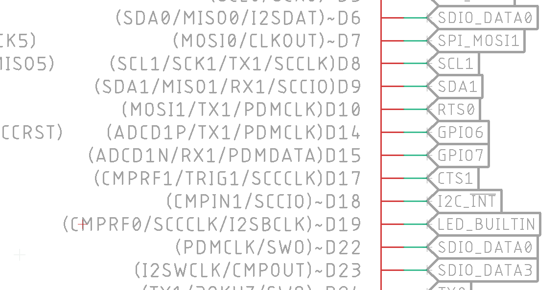
If your processor supports SDIO connect it to the MicroMod SDIO pins. If the SPI1 pins are different than the SDIO pins then consider connecting both signals together. For example, on Artemis (shown below) the MOSI0 pin (pin D6) is being used as part of SPI1. Pin D22 is SDIO_DATA0. By connecting both MISO0 and D22 to SDIO_DATA0 on the MicroMod connector the user has the ability to either use SDIO or SPI (one pin D6/D22 will be high impedance). And, the real benefit, the user can route the full SDIO interface/pins to a microSD socket on a carrier board. If the MicroMod processor board does not have library support for SDIO (most don’t) then the user can fall back to using SPI to talk to the microSD card (almost all platforms have support for this)
Artemis with SDIO_DATA0 connected to two pins.
MicroSD socket on a carrier board wired to support both SDIO and SPI.

Routing
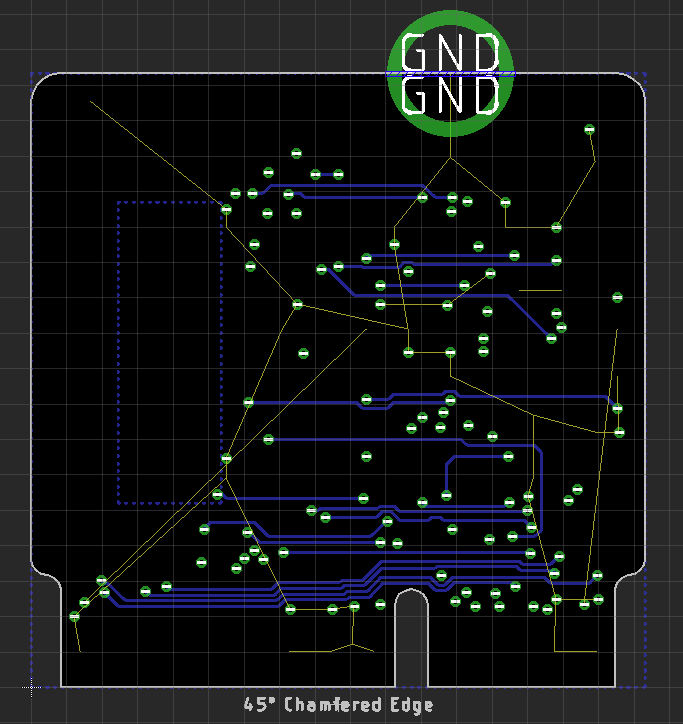
MicroMod PBs are 4-layer boards, 0.8mm thickness, ENIG finish (for the gold fingers) with a 20° edge bevel.
 |
 |
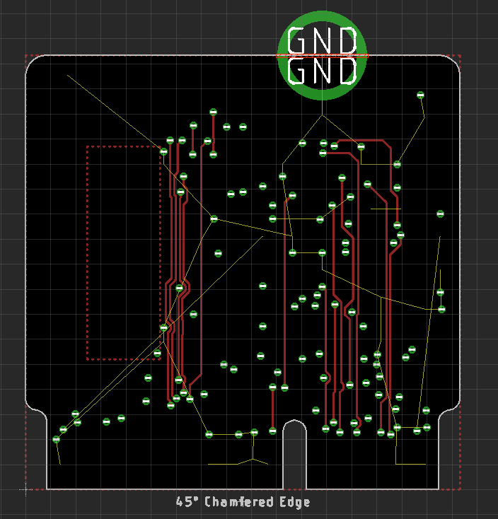 |
- Place components on both sides of the board.
- In general, the main processor goes on the ‘front’. This is the side that will face up at the user.
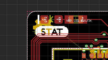
Status LEDs
Place the ‘STAT’ LED in the upper left or upper right corner. If that’s not possible, place near the upper edge.
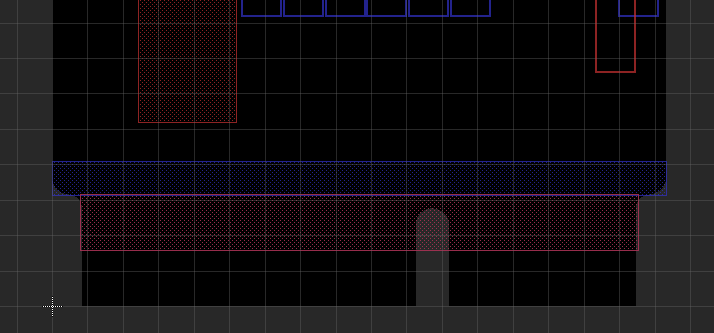
Keep Out Layer for M.2 Edge Connector Specification
Heed the top and bottom keepout areas near the edge of the PB. These are part of the M.2 spec and are related to how the card edge interacts with the connector.
Eagle Layer Setup Commands and Hotkeys
Setup Eagle for four layers with the following command:
Set Used_Layers 1 2 15 16 17 18 19 20 21 22 23 24 25 26 27 28 29 30 31 32 33 34 35 36 37 38 39 40 41 42 43 44 45 46 47 48 49 50 51 52 91 92 93 94 95 96;
And if you need it, this is how to go back to 2 layers:
Set Used_Layers 1 16 17 18 19 20 21 22 23 24 25 26 27 28 29 30 31 32 33 34 35 36 37 38 39 40 41 42 43 44 45 46 47 48 49 50 51 52 91 92 93 94 95 96;
I have edited my eagle.scr to quickly view the internal layers by themselves. This is helpful during routing.
#Used for four layer routing
DISPLAY = VerticalOnly 15 17 18 19 20;
DISPLAY = HorizontalOnly 2 17 18 19 20;
Assign A+0 'display none; display VerticalOnly;'
Assign A+9 'display none; display HorizontalOnly;'
This sets an Alt+0 hotkey that views only layer 15 (vertical routes shown in red above) and Alt+9 that views only layer 2 (horizontal routes shown in blue above). We can add this to the Eagle settings repo if people like it or have a better recommendation.
Trace Width, Trace Spacing, Drill Hits
Routing Processor Boards is tricky. There’s no way around it. Luckily, we can use some very tight tolerances. Use 0.004” traces with 0.0045” space. Use 0.2mm drill hits. Route vertically on layer 15 and horizontally on 2. This will reduce the chance of cross talk on high speed signals. Traces as small as 3.5mil with 3.5mil space ARE allowed and basically free. But going this small increases the chance of cross talk so be wary.
It is recommended to use layer 2 as ground and layer 15 as 3.3V. This will help with PBs that have microstrip RF traces that need a close proximity to a ground plane to minimize the width of a 50 ohm trace.
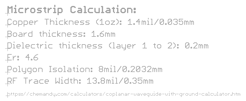
Microstrip
Does your PB have a microstrip? See Qwiic-GPS-RTK2 hardware repo for an example of 4 layer microstrip and the settings JLCPCB uses for Er and layer stackup. Note: RTK2 was a 1.6mm thick board and PBs are 0.8mm so adjust the numbers as necessary.
Call the device ‘MicroMod Blarg’, not the reverse.
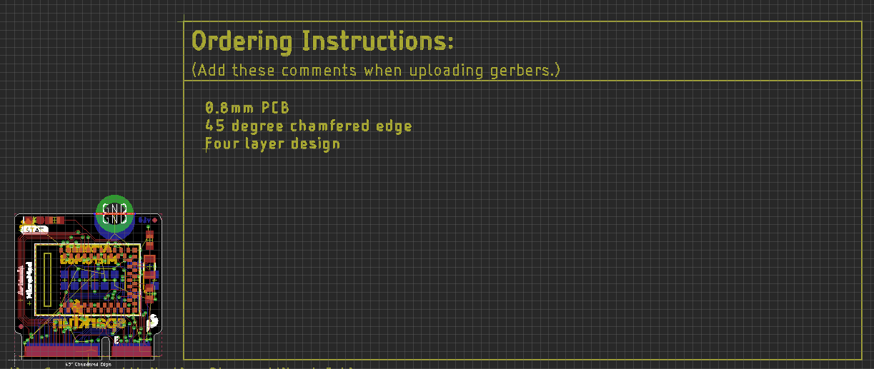
Be sure to include special ordering instructions on your design:
- 0.8mm board thickness
- 45 degree chamfered edge
- Four layer design
Fabrication
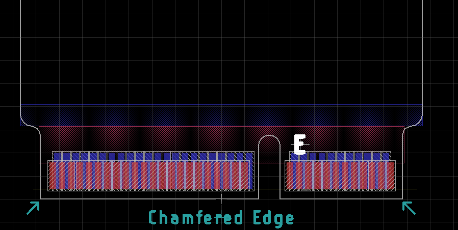
The M.2 spec calls for a 20° bevel on the card edge. However, it seems most PCB fab houses are setup for a 45° bevel, and they like to call it a ‘chamfered’ edge. After testing a few runs of boards, 45° chamfer works great. To date, we have not tested a board that does not have a bevel on the card edge. I suspect it will still work, but insertion into the connector may feel different. The text ‘Chamfered Edge’ is automatically added to the panel via the footprint.
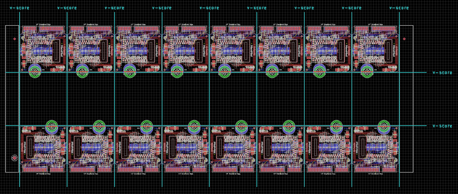
We have modified the SparkFun panelizer (read more here, and get the latest files here) to create panels capable of getting the edges beveled.
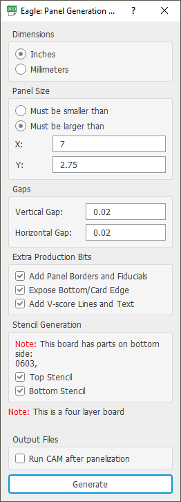
Be sure to select ‘Expose Bottom/Card Edge’. Y must be 2.75” or greater, otherwise the fab house cannot v-score. X can be 3” or more. We have found that the price of the PCB doesn’t change much from 3” to 7”. Our SMD line handles panels up to ~9” so that's what we often go with. Note: The panelizer will replicate the DRC settings from the original design.
A panel ready for CAM and then fab.
Manufacturing
Most orders for 10 panels, 4 layer, 4mil trace/space, gold fingers, ENIG finish, with beveled edge, cost ~$100 with ~$20 in shipping from JLCPCB. We've found the fab times to be ~8 days but vary. Either way, this is extraordinarily cheap and pretty fast.
For this scale of design, a stainless steel stencil is a must (no mylar). If your assembly process allows for framed stencils, go ahead and get one. Hand stenciling is difficult with the scale of PBs’ 0402 components and tight placements.