Designing with MicroMod
Introduction
This tutorial will walk you through the specs of the MicroMod processor and carrier board as well as the basics of incorporating the MicroMod form factor into your own PCB designs!
 |
 |
Suggested Reading
If you aren’t familiar with the following concepts, we recommend checking out these tutorials before continuing.
PCB Basics
Using EAGLE: Board Layout
Getting Started with MicroMod
How to Design a MicroMod Processor Board
Instead of starting from scratch, we'll start with a known good development board. In this case, we'll start with a development board and convert it to a MicroMod Processor Board (PB).
Schematic
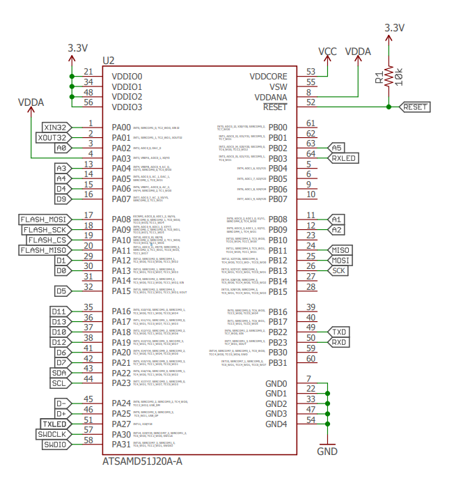
Start with a known good development board product, the SAMD51 Thing Plus for example, and remove all the bits from the EAGLE design that are not needed from the schematic:
- USB connector
- Qwiic connector
- JST connector
- Standoffs
- Headers
- Power regulation
- Reset buttons
- Silk
- TX/RX LEDs
- Battery charging
Keep any needed external circuitry such as:
- Decoupling
- ADC amplification
- Crystals for main clock of RTC
- External memory to enable Python script loading
- 1 status LED (usually connected to LED_BUILTIN)
- USB to serial conversion IC and circuitry
Keep anything needed for the device to be programmed by only USB +/-. This means you may need to include a USB to serial IC (CH340E is recommended) for devices that don’t have built-in USB peripherals. Retain any boot control circuitry (Artemis and ESP32 have boot pins that need to be controlled by RTS/DTR).
Remove all LED indicators that will be relocated to the carrier board. This includes TX/RX LEDs, Power LEDs, charge LEDs, etc. The exception to this is every Processor Board shall include one status LED connected to a pin that is not connected to the board edge. This enables the user to immediately test their processor board agnostic of the capabilities of the carrier board.
Check to see if there have been any changes or improvements to the general design using this processor. For a hypothetical example, users may be populating the SAMD51 boards with a 32mbit flash as opposed to the older 16mbit flash. Roll these improvements into the design.
Now is your chance to clean up the schematic component for the processor. Combine duplicate GND pins, VDDIO pins, etc into single pins on the schematic component.
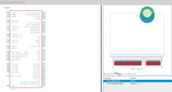
Pull in the MicroMod card edge connector from the SparkFun Eagle library. You'll find it under 'SparkFun-MicroMod'.
In the schematic, begin connecting the various dedicated hardware pins on the microcontroller to the MM card edge. For example, on the SAMD51:
- Connect USB +/- on processor to USB +/- on MM edge connector
- Primary I2C pins on SAMD51 connect to primary I2C pins on MM
- Flash pins go to onboard flash (no move)
- SPI pins go to primary SPI pins on MM
- TX/RX go to TX1/RX1 on MM
- RX LED, TX LED connections get removed entirely
- The reset pin on MM is defined as an output open drain. The CB will have a reset button. So be sure to keep the pull up on reset on the PB.
- Does this processor need special boot pin controls? The Boot pin is input open drain. The carrier board can have a ‘boot’ button that pulls this pin low. Invert this signal and/or add circuitry as needed to work with this processor if needed.
- Does this processor support SWD? Connect SWDIO and SWCK as needed.
- Does this processor have differential ADC capabilities? If so, connect the differential ADC pins to ADC+/- (G9/10).
- Are there any pins on this processor capable of I2S, PDM, CAN, or USB host? * Be sure to connect those and give them priority over the general ADC, PWM, GPIO connections.
- Dedicate one ADC capable pin to BATT_VIN/3. This pin will read the VIN voltage through a ⅓ voltage divider located on the CB.
- Dedicate one GPIO to 3.3V_EN. This allows the PB to turn off the main voltage regulator on the CB. This is a dicey pin that needs thinking. Only processors that can sleep and wakeup from RTC / low power battery backup should be able to turn off the main CB voltage regulator.
- Route any power from RTC_3V on the edge connector to any pins on the processor that need power from a coin cell or mini battery to run the RTC.
- Does this processor support a Clock Out or special clock generation pin (output)? If so, connect to the AUD_OUT/CAM_MCLK pin.
Now it’s time to make some architecture decisions:
- Are there other peripherals that can be exposed on the SAMD51 to the card edge? For example, SAMDs have flexible SERCOM ports. Should we dedicate some unused IO to a 2nd SPI port? 2nd UART? 2nd I2C?
- Once dedicated hardware is roughed out and connected, find pure analog capable pins. Connect those to A0 and A1.
- Next, find pins that are purely PWM capable pins. Connect those to PWM0 and PWM1.
- Next, find pins that are purely GPIO capable pins (no ADC or PWM). Connect those to D0 and D1.
- Next, find pins that are bus capable, aka ‘fast write’ capable. For example PB00 to PB07 can be accessed with single register read/writes.
- Any remaining pins should be assigned to Gx with ADC + PWM capable pins given priority (0, 1, 2, etc) positions. The intent is to guarantee PWM, ADC, and Digital Pin functionality on those specific pins (A0, D1, PWM1, etc). Whereas Gx pins do not guarantee ADC/PWM function.
- Any remaining GPIO can be routed to the unused secondary interfaces. For example, if SAMD51 doesn’t have a 2nd I2C port then these pins can be connected to GPIO.
Antennas
The processor board should include any trace or chip antenna to support the functionality of the processor. If the application makes sense, add a U.FL connector.
SDIO and SPI1 Pins
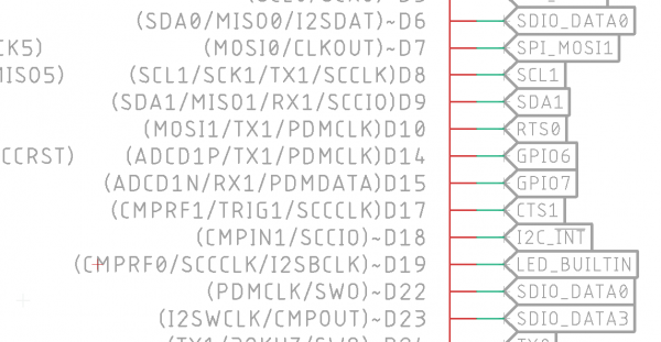
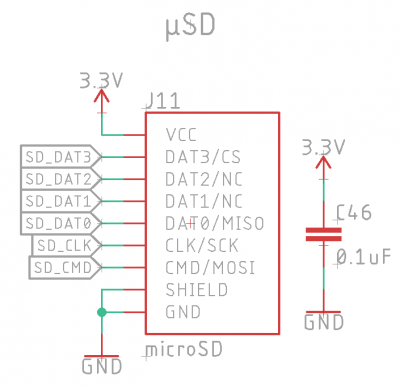
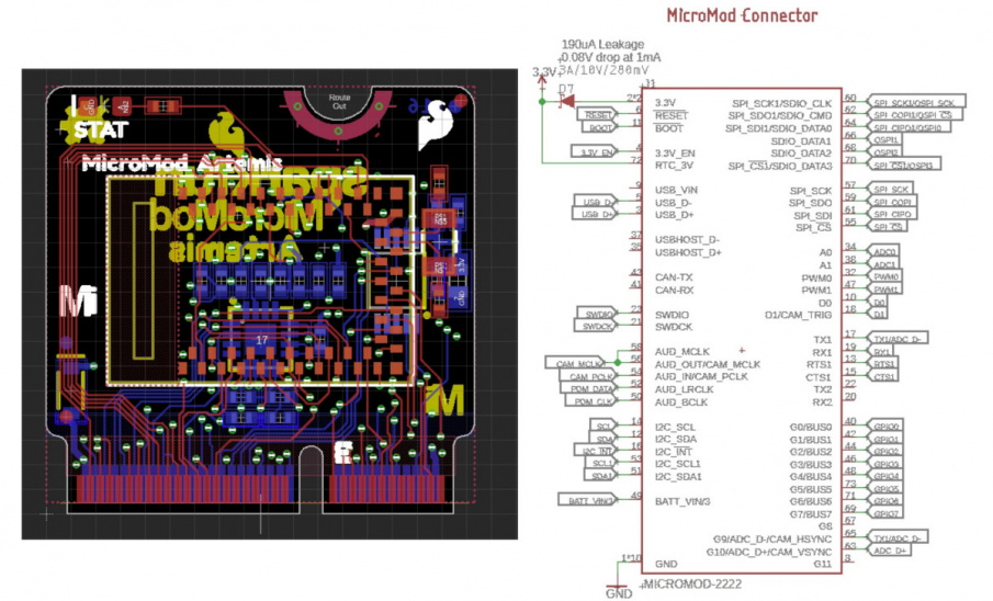
If your processor supports SDIO connect it to the MicroMod SDIO pins. If the SPI1 pins are different than the SDIO pins then consider connecting both signals together. For example, on Artemis (shown below) the MOSI0 pin (pin D6) is being used as part of SPI1. Pin D22 is SDIO_DATA0. By connecting both MISO0 and D22 to SDIO_DATA0 on the MicroMod connector the user has the ability to either use SDIO or SPI (one pin D6/D22 will be high impedance). And, the real benefit, the user can route the full SDIO interface/pins to a microSD socket on a carrier board. If the MicroMod processor board does not have library support for SDIO (most don’t) then the user can fall back to using SPI to talk to the microSD card (almost all platforms have support for this)
Artemis with SDIO_DATA0 connected to two pins.
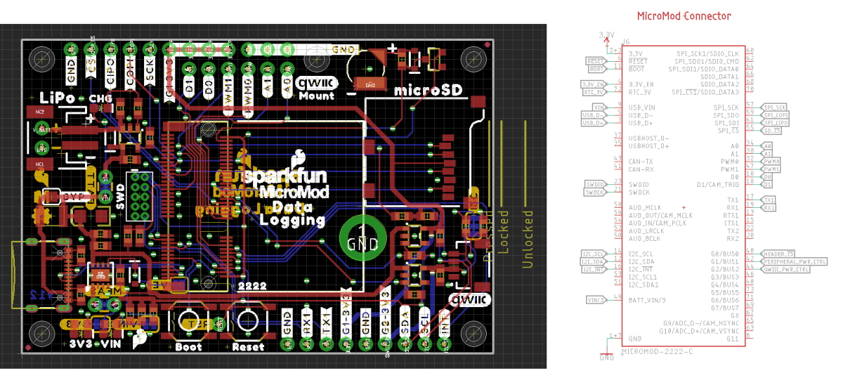
MicroSD socket on a carrier board wired to support both SDIO and SPI.
Routing
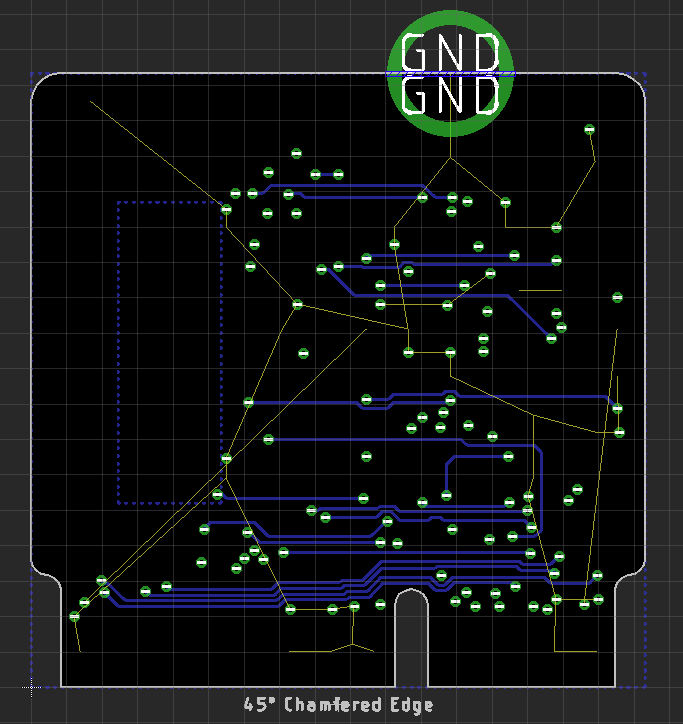
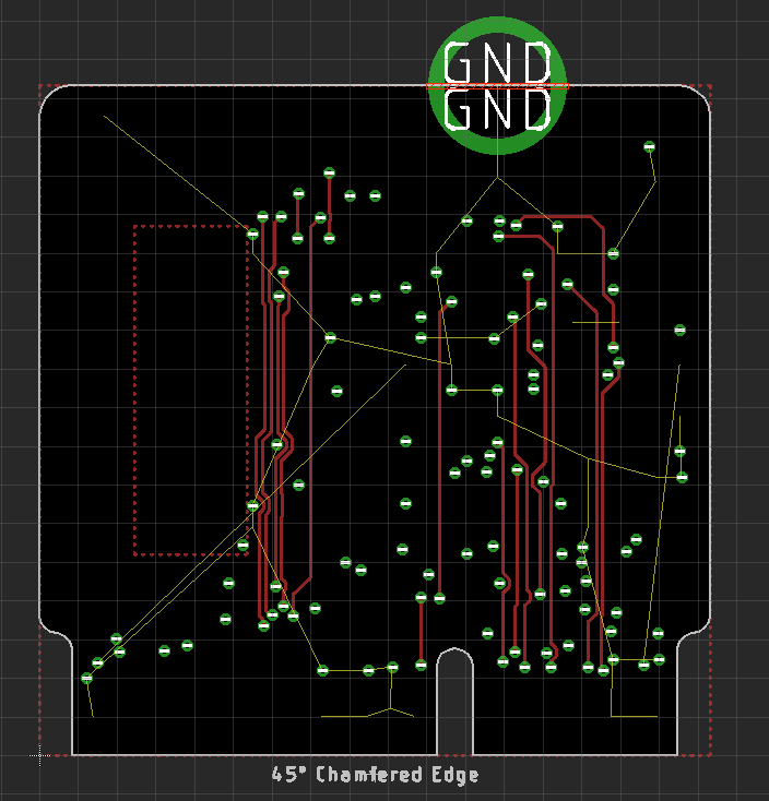
MicroMod PBs are 4-layer boards, 0.8mm thickness, ENIG finish (for the gold fingers) with a 20° edge bevel.
 |
 |
 |
- Place components on both sides of the board.
- In general, the main processor goes on the ‘front’. This is the side that will face up at the user.
Status LEDs
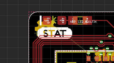
Place the ‘STAT’ LED in the upper left or upper right corner. If that’s not possible, place near the upper edge.
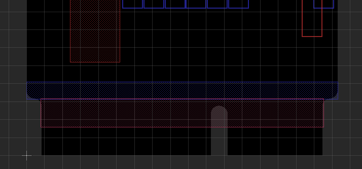
Keep Out Layer for M.2 Edge Connector Specification
Heed the top and bottom keepout areas near the edge of the PB. These are part of the M.2 spec and are related to how the card edge interacts with the connector.
Eagle Layer Setup Commands and Hotkeys
Setup Eagle for four layers with the following command:
Set Used_Layers 1 2 15 16 17 18 19 20 21 22 23 24 25 26 27 28 29 30 31 32 33 34 35 36 37 38 39 40 41 42 43 44 45 46 47 48 49 50 51 52 91 92 93 94 95 96;
And if you need it, this is how to go back to 2 layers:
Set Used_Layers 1 16 17 18 19 20 21 22 23 24 25 26 27 28 29 30 31 32 33 34 35 36 37 38 39 40 41 42 43 44 45 46 47 48 49 50 51 52 91 92 93 94 95 96;
I have edited my eagle.scr to quickly view the internal layers by themselves. This is helpful during routing.
#Used for four layer routing
DISPLAY = VerticalOnly 15 17 18 19 20;
DISPLAY = HorizontalOnly 2 17 18 19 20;
Assign A+0 'display none; display VerticalOnly;'
Assign A+9 'display none; display HorizontalOnly;'
This sets an Alt+0 hotkey that views only layer 15 (vertical routes shown in red above) and Alt+9 that views only layer 2 (horizontal routes shown in blue above). We can add this to the Eagle settings repo if people like it or have a better recommendation.
Trace Width, Trace Spacing, Drill Hits
Routing Processor Boards is tricky. There’s no way around it. Luckily, we can use some very tight tolerances. Use 0.004” traces with 0.0045” space. Use 0.2mm drill hits. Route vertically on layer 15 and horizontally on 2. This will reduce the chance of cross talk on high speed signals. Traces as small as 3.5mil with 3.5mil space ARE allowed and basically free. But going this small increases the chance of cross talk so be wary.
It is recommended to use layer 2 as ground and layer 15 as 3.3V. This will help with PBs that have microstrip RF traces that need a close proximity to a ground plane to minimize the width of a 50 ohm trace.
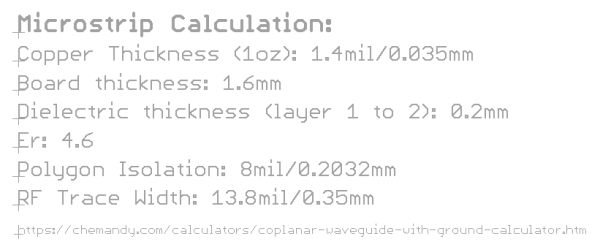
Microstrip
Does your PB have a microstrip? See Qwiic-GPS-RTK2 hardware repo for an example of 4 layer microstrip and the settings JLCPCB uses for Er and layer stackup. Note: RTK2 was a 1.6mm thick board and PBs are 0.8mm so adjust the numbers as necessary.
Call the device ‘MicroMod Blarg’, not the reverse.
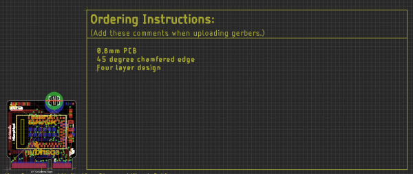
Be sure to include special ordering instructions on your design:
- 0.8mm board thickness
- 45 degree chamfered edge
- Four layer design
Fabrication
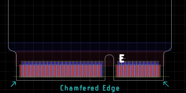
The M.2 spec calls for a 20° bevel on the card edge. However, it seems most PCB fab houses are setup for a 45° bevel, and they like to call it a ‘chamfered’ edge. After testing a few runs of boards, 45° chamfer works great. To date, we have not tested a board that does not have a bevel on the card edge. I suspect it will still work, but insertion into the connector may feel different. The text ‘Chamfered Edge’ is automatically added to the panel via the footprint.
We have modified the SparkFun panelizer (read more here, and get the latest files here) to create panels capable of getting the edges beveled.
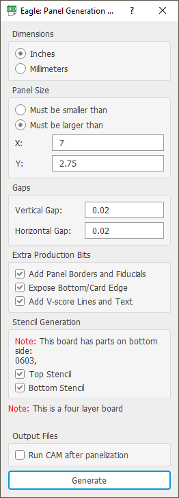
Be sure to select ‘Expose Bottom/Card Edge’. Y must be 2.75” or greater, otherwise the fab house cannot v-score. X can be 3” or more. We have found that the price of the PCB doesn’t change much from 3” to 7”. Our SMD line handles panels up to ~9” so that's what we often go with. Note: The panelizer will replicate the DRC settings from the original design.
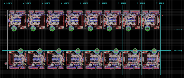
A panel ready for CAM and then fab.
Manufacturing
Most orders for 10 panels, 4 layer, 4mil trace/space, gold fingers, ENIG finish, with beveled edge, cost ~$100 with ~$20 in shipping from JLCPCB. We've found the fab times to be ~8 days but vary. Either way, this is extraordinarily cheap and pretty fast.
For this scale of design, a stainless steel stencil is a must (no mylar). If your assembly process allows for framed stencils, go ahead and get one. Hand stenciling is difficult with the scale of PBs’ 0402 components and tight placements.
How to Design a MicroMod Carrier Board
Start with a known good carrier board; the MicroMod Machine Learning Carrier Board is a good example.
The core of the carrier board is the MicroMod M.2 connector, standoff and screw.
We carefully designed the standoff to be reflowable and compatible with the 4.2mm high M.2 connector so that carrier boards can have a limited number of components underneath the Processor Board. Additionally, the screw was chosen to be slightly larger (M2.5) with a Phillips head so that users will have the best experience possible. We recommend checking that you have a #00, #0, or #1 Phillips head driver available. If not, our classic SparkFun reversible mini-screw driver or the fancier pocket screw driver set work great.
For those folks that don't use EAGLE the datasheets including footprints follow:
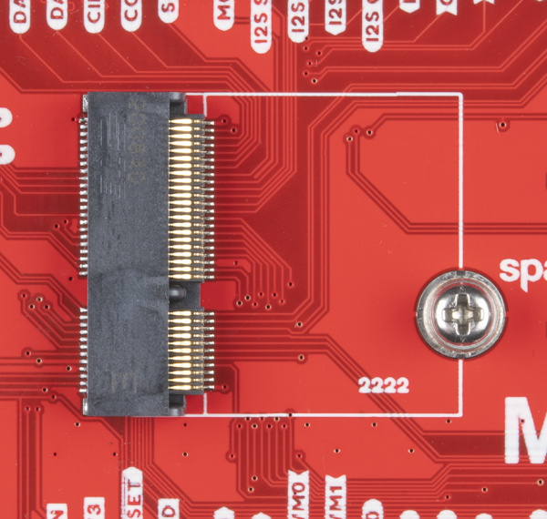
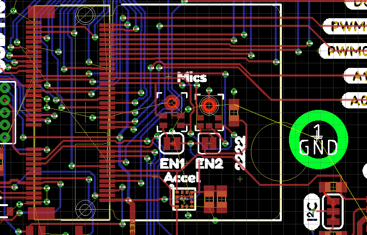
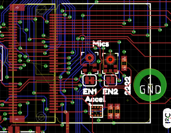
Open up the SparkFun Eagle library and navigate to the 'SparkFun-MicroMod' library. The SMD reflowable standoff is a separate component (found in the 'SparkFun-Hardware' library) from the MicroMod connector so that we can track the parts correctly in Sparkle (the SparkFun's in house ERP system). The connector has a circle where the standoff needs to fall. It needs to be close but not micron perfect. We currently plan to only have 22x22mm MicroMods Processor Boards (note the ‘2222’ text) but this may grow in the future.
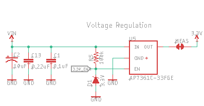
We currently recommend using the AP7361C 3.3V 1A linear regulator. In addition, please include the zener and pullup on the enable pin. This allows a MicroMod Processor Board to turn off the main power supply when necessary, enabling considerable power savings. The zener protects the MicroMod Processor Board from damage to its GPIO from VIN.
Note the MEAS jumper below. This allows for cutting and inline current measuring. Note the BYP jumper. This allows the user to bypass the PTC and increase current use beyond 2A PTC cut off if supported by their power supply.
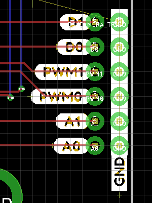
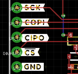
Interface pins should be grouped together but their location on the board is not specified.
 |
 |
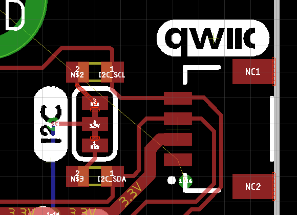
A Qwiic connector with pullups and a logo should be put on every carrier board. Note the thick 0.022” 3.3V trace enabling 2A delivered to the Qwiic bus.
Components under the MicroMod Processor Board are allowed. Be careful of component height! Any component placed under MicroMod with 4.2mm height connector (the standard connector we stock) must be less than 1.9mm +/-0.1mm tall. No Artemis (too tall), yes SOT-23-5, yes CH340C/E. Double check the height of the components on the bottom of all MicroMod Processor Boards.
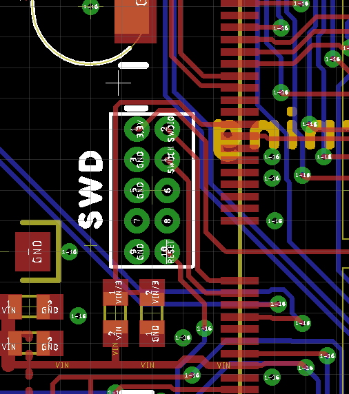
All carrier boards should have a Serial Wire Debug (SWD) port. Not all processor support SWD but many do.
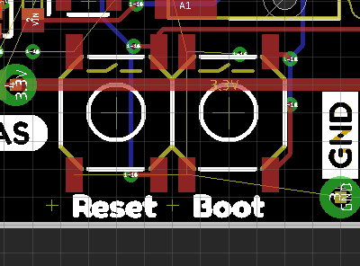
Add a reset button and consider adding a boot button. Currently, the boot input is not utilized on many Processor Boards but should be included for future use. We prefer the SMD button with the 5.2mm actuator (feels great!).
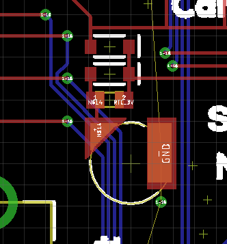
Consider adding RTC/low power backup to your board. The RTC backup battery configuration shown is pretty well tested. It’s compact, SMD compatible, and provides 1mAh of capacity. Your application may be high power (a motor driver) where RTC doesn’t make sense. It’s ok to leave off.
Now add anything you may need to your carrier board for your specific application. LiPo charging, DB9, RFID, whatever. The power of MicroMod and the challenge to you is to consider how your added peripherals are going to play with the various MicroMod Processor Boards. Adding a serial device is straightforward, most all Processor Boards will have TX/RX1. Adding a PDM microphone or 4 bit high speed (Quad SPI) display takes more consideration.
Routing is straightforward. Match the length of any high speed traces such as USB D+/D-, USB HOST D+/D-. Consider using 7mil trace/space with 0.012” drills. Ues 0.022” traces for up to 2A power buses. Smaller traces down to 0.0035mil and 0.2mm drills are allowed but highly unlikely we’ll need it. Four layer boards are cheap these days but again, highly unlikely we’ll need it. Carrier boards should be much less complex because all the complexity should be pushed into the Processor Board.
Pull-ups on Chip Select (CS) pins: Pull-ups live with the peripheral. So if the carrier board has a SPI device on the board (SD, sensor, etc), that device needs to have a pull up on the CS pin. If the CS line is simply brought out to a PTH header on the edge of a board it does not need a pull-up (that pull-up should live on the peripheral that gets soldered to the SPI pins). Use a 100k where possible but the value can be changed as the peripheral’s datasheet specifies.
How to Design a Function Board
What's in a Function Board?
A Function Board is a modular PCB made to plug into an M.2 connector. Similar in theory to the Processor board (plug and play), but targeted at peripherals for the processor board. The function boards are made to interconnect with Processor Boards on a larger main board. This creates an ecosystem in which no soldering iron is required for multiple embedded systems to interact smoothly and efficiently.
Physical Dimensions and Layout
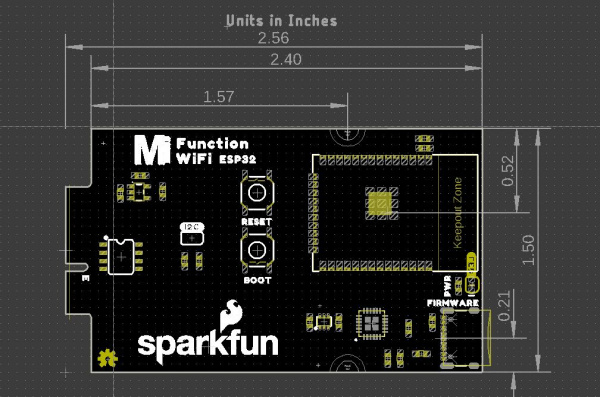
The Function Board comes in a single size that is 65mm X 38mm (2.56" x 1.5"). The PCB inserts into a M.2 connector and as a result is 0.8mm thick, half the thickness of a standard PCB.
 |
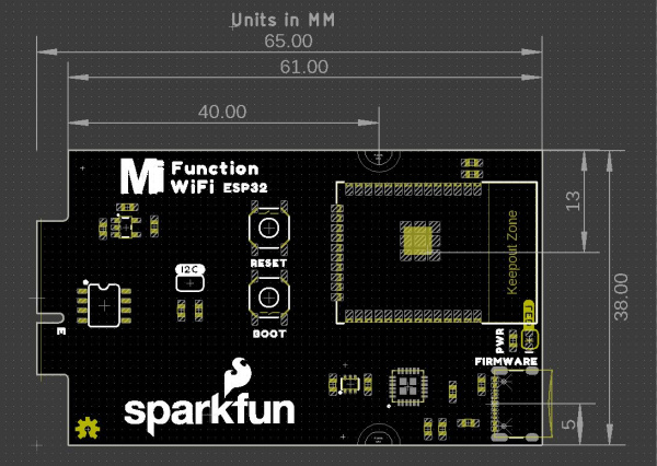 |
| Dimensions in Inches | Dimensions in Millimeters |
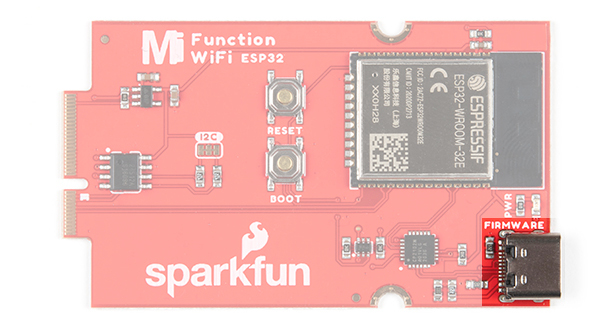
The edge opposite the card edge always includes any connectors needed by the Function Board. For example, the WiFi Function Board includes a USB-C connector for uploading AT Command Firmware to the ESP32; the LoRa board includes an SMA connector for an antenna.
This helps with ease of use, but also for placing a Function with in a case. Speaking of ease of use, connectors should sit at some measurement within the Function board's PCB that doesn't require five decimal points of precision.
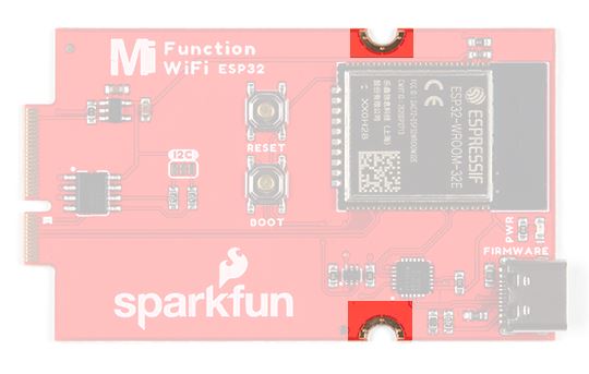
There are and must be at least two standoffs for securing the Function Board down to keep the board from moving when plugging in cables on the card edge.
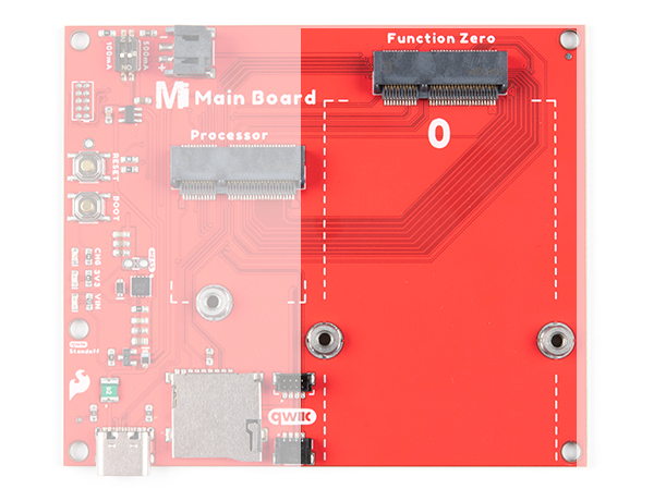
You can see the complementary female standoffs on the Main Board - Single that secure the Function Board to the PCB.
M.2 Card Pinout
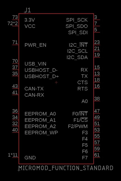
The M.2 pinout includes many of the major buses: Serial Peripheral Interface (SPI), Inter-Integrated Circuit (I2C), Serial, USB Host, and the Control Area Network (CAN) Bus. There are eight digital pins with a number of dedicated overlapped functionalities at the lower enumerated pin numbers. For example F0 is a dedicated interrupt, F1 includes a dedicated Chip Select pin for the SPI bus, and F2 is a dedicated Pulse Width Modulation (PWM) pin. Aside from the general purpose pins, there is a single analog pin A0 and finally, a power enable pin. The power enable pin's intended use is to allow power to the function board to be easily switched on and off. On SparkFun's Function boards we simply use popcorn voltage regulators to facilitate power, passing the power enable pin to the card's edge, making it easy to shut off power.
The MicroMod Function Board symbol and footprint can be found within the SparkFun Eagle Libraries Repository within the SparkFun-Micromod.lib. The device name is MicroMod-Function which includes the Function Board under the "MICROMOD-FUNCTION-STANDARD" variant, and the M.2 connector under the "MICROMOD-FUNCTION-MAIN" variant.
The Parts
This might go without saying, but the Function Board should have all the included parts necessary to support any ICs on it. For example, if the intention is for the Function Boards to be a datalogger, consider putting an SD Card socket on it.
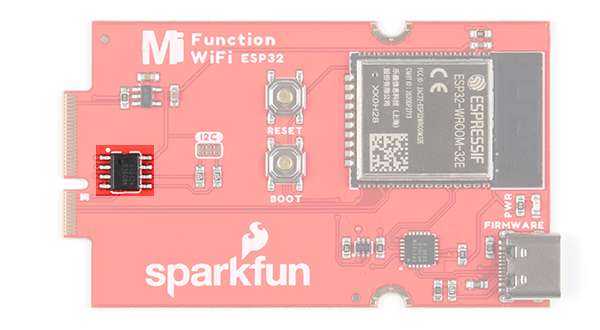
Additionally we've included an EEPROM on each of the Function Boards and it contains basic information about the Function Board.
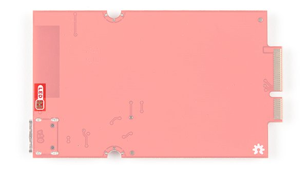
The MicroMod ecosystem always wants to support low power applications as much as possible. If your Function Board has any LEDs than include jumpers to remove power from them.
Pin Specifications
The MicroMod interface is defined as follows:
Useful component datasheets:
Here is the pinout description information in table form:
| Signal Group | Signal | I/O | Description | Voltage |
|---|---|---|---|---|
| Power | 3.3V | I | 3.3V Source | 3.3V |
| GND | Return current path | 0V | ||
| USB_VIN | I | USB VIN compliant to the USB 2.0 Specification. Connect to any pins on the processor that require 5V for USB functionality. | 4.8-5.2V | |
| RTC_3V_BATT | I | 3V provided by external coin cell or mini battery. Max draw = 100uA. Connect to pins that maintain an RTC during power loss. Can be left NC. | 3V | |
| 3.3V_EN | O | Controls the carrier board's main voltage regulator. Voltages above 1V will enable 3.3V power path. Can be left NC. If implemented, carrier board must supply pullup resistor and 3.3V clamping on regulator enable pin. | 3.3V | |
| BATT_VIN/3 | I | Carrier board raw voltage over 3. 1/3 resistor divider is implemented on carrier board. Amplify the analog signal as needed to enable full 0-3.3V range. | 3.3V | |
| Reset | Reset | I | Input to processor. Open drain with pull up on processor board. Pulling low resets processor. | 3.3V |
| Boot | I | Input to processor. Open drain with pull up on processor board. Pulling low puts processor into special boot mode. Can be left NC. | ||
| USB | USB_D+ USB_D- |
I/0 | USB Data ± Differential serial data interface compliant to the USB 2.0 specification. If a UART is required for programming, USB+/- must be routed to a USB-to-serial conversion IC on the processor board. | |
| USB_HOST | USBHOST_D+ USBHOST_D- |
I/0 | For processors that support USB Host Mode. USB Data ± differential serial data interface compliant to the USB 2.0 specification. Can be left NC. | |
| CAN | CAN_RX | I | CAN Bus Receive Data | 3.3V |
| CAN_TX | O | CAN Bus Transmit Data | 3.3V | |
| UART | UART_RX1 | I | UART Receive Data | 3.3V |
| UART_TX1 | O | UART Transmit Data | 3.3V | |
| UART RTS1 | O | UART Ready to Send | 3.3V | |
| UART CTS1 | I | UART Clear to Send | 3.3V | |
| UART_RX2 | I | 2nd UART Receive Data | 3.3V | |
| UART_TX2 | O | 2nd UART Transmit Data | 3.3V | |
| Note: UART1/2 must be unencumbered (not attached to a USB-to-serial conversion IC). | ||||
| Note: UART0 is not shown. Primary debug serial is done over USB. Serial.print() should print over USB, not TX1. | ||||
| I2C | I2C_SCL | I/O | I2C Clock. Open drain with pull up on carrier board. | 3.3V |
| I2C_SDA | I/O | I2C Data. Open drain with pull up on carrier board. | 3.3V | |
| I2C_INT# | I | Interrupt notification from carrier board to processor. Open drain with pull up on carrier board. Active Low. | 3.3V | |
| I2C_SCL1 | I/O | 2nd I2C Clock. Open drain with pull up on carrier board. | 3.3V | |
| I2C_SDA1 | I/O | 2nd I2C Data. Open drain with pull up on carrier board. | 3.3V | |
| SPI/SDIO | SPI_SCK SDIO_CLK |
O | SPI Clock. Secondary use: SDIO Clock. | 3.3V |
| SPI_COPI SDIO_CMD |
IO | SPI Controller Out Peripheral In. Secondary use: SDIO Command Interface. | 3.3V | |
| SPI_CIPO SDIO_DATA0 |
I/O | SPI Controller In Peripheral Out. Secondary use: SDIO data exchange bit 0. | 3.3V | |
| SDIO_DATA1 | I/O | SDIO data exchange bit 1 | 3.3V | |
| SDIO_DATA2 | I/O | SDIO data exchange bit 2 | 3.3V | |
| SPI_CS SDIO_DATA3 |
I/O | SPI Chip select. Active low. Secondary use: SDIO data exchange bit 3. | 3.3V | |
| Note: The carrier board SD socket can fall back to SPI if lines are routed correctly. Connect multiple pins to obtain dual function as necessary. For example, if CIPO1 is a different pin from DATA0 on processor, then route both CIPO1 and DATA0 to SDIO_DATA0 on board edge. | ||||
| SPI_CIPO1 | I | 2nd SPI Controller In, Peripheral Out | 3.3V | |
| SPI_COPI1 | O | 2nd Controller Out, Peripheral In | 3.3V | |
| SPI_SCK1 | O | 2nd SPI clock | 3.3V | |
| SPI_CS#1 | O | 2nd SPI chip select. Active low. Can be routed to GPIO if hardware CS is not used. | 3.3V | |
| AUDIO | AUD_MCLK | O | Audio Master Clock | 3.3V |
| AUD_OUT PCM_OUT I2S_OUT CAM_MCLK |
O | Audio data output. PCM synchronous data output. I2S serial data out. Camera master clock. | 3.3V | |
| AUD_IN PCM_IN I2S_IN CAM_PCLK |
I | Audio data input. PCM synchronous data inut/I2S serial data in. Camera peripheral clock. | 3.3V | |
| AUD_LRCLK PCM_SYNC I2S_WS PDM_DATA |
I/O | Audio left/right clock. PCM synchronous data SYNC. I2S word select. PDM data. | 3.3V | |
| AUD_BLCK PCM_CLK I2S_SCK PDM_CLK |
O | Audio bit clock. PCM clock. I2S continuous serial clock. PDM clock. | 3.3V | |
| SWD | SWDIO | I/O | Serial Wire Debug I/O. Connect if processor supports SWD. Can be left NC. | 3.3V |
| SWDCK | I | Serial wire debug clock. Connect if processor supports SWD. Can be left NC. | 3.3V | |
| ADC | A0 | I | Analog to digital converter 0. Amplify the analog signal as needed to enable full 0-3.3V range. | 3.3V |
| A1 | I | Analog to digital converter 1. Amplify the analog signal as needed to enable full 0-3.3V range. | 3.3V | |
| PWM | PWM0 | O | Pulse width modulated output 0. | 3.3V |
| PWM1 | O | Pulse width modulated output 1. | 3.3V | |
| Digital | D0 | I/O | General digital input/output pin. | 3.3V |
| D1 CAM_TRIG |
I/O | General digital input/output pin. Camera trigger. | 3.3V | |
| GPIO/BUS | G0/BUS0 | I/O | General purpose pins. Any unused processor pins should be assigned to Gx with ADC + PWM capable pins given priority (0, 1, 2, etc) positions. The intent is to guarantee PWM, ADC, and digital pin functionality on ADC/PWM/Digital specific pins. Whereas Gx pins do not guarantee ADC/PWM function. Alternatively, pins can be used to support a fast read/write 8-bit wide or 4-bit wide bus. | 3.3V |
| G1/BUS1 | I/O | 33V | ||
| G2/BUS2 | I/O | 3.3V | ||
| G3/BUS3 | I/O | 3.3V | ||
| G4/BUS4 | I/O | 3.3V | ||
| G5/BUS5 | I/O | 3.3V | ||
| G6/BUS6 | I/O | 3.3V | ||
| G7/BUS7 | I/O | 3.3V | ||
| G8 | I/O | General purpose pin. | 3.3V | |
| G9 ADC_D- CAM_HSYNC |
I/O | Differential ADC input if available. Camera horizontal sync. | 3.3V | |
| G10 ADC_D+ CAM_VSYNC |
I/O | Differential ADC input if available. Camera vertical sync. | 3.3V | |
| G11 SWO |
I/O | General purpose pin. Serial Wire Output. | 3.3V | |
Resources and Going Further
For more information, check out the resources below:
- SparkFun MicroMod Interface v1.0 - Pinout
- SparkFun MicroMod Interface v1.0 - Pin Descriptions
- SparkFun Eagle Libraries contains example footprints for the M.2 connector and SMD standoff
- M.2 MicroMod Connector Datasheet
- M2.5 Reflowable Standoff Datasheet
- MicroMod Info Page
- MicroMod Forums
Looking for more MicroMod fun? Check out the following tutorials with MicroMod for more inspiration!
