BC118 BLE Mate 2 Hookup Guide
 SFUptownMaker
Hardware Connection
This page will cover both general hardware connection for the BLE Mate 2 as well as specific information for this tutorial.
6-pin Serial Header
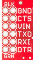
The pinout on this header matches that of the FTDI Basic boards, so it can be used anywhere an FTDI basic can be. However, it's probably not fast enough to do any kind of wireless bootloading.
- DTR - Connected only to the other DTR pad. This pin can be connected to PIO5 to provide a DTR output to the client device; that signal will be at a voltage determined by the supply voltage of the BC118 module and so may not be adequate to drive the reset signal on an Arduino.
- RXI - Data IN from the client device.
- TDO - Data OUT from the BC118 device. Shifted up to the level on the VCC pin of this header.
- VCC - Connected to the INP jumper (see below).
- CTS - Connected only to the other CTS pad. Can be connected to PIO6 to provide an RTS signal to the BC118. That signal must not exceed the supply voltage of the BC118 module.
- GND - Negative supply rail for the entire module.
GPIO Headers
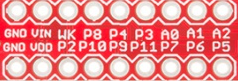
There are two 0.1" (2.54mm) headers along the sides of the module. These pins are 0.9" (22.5mm) apart, so they'll fit into a breadboard (although not a lot of space will be left outside the pins!)
The currently useful pins on the BC118 module are all broken out to these headers; I'll go over what they do and what they can do. Here, I'll talk about commands and configuration parameters on the next page, but they will be referenced below.
- **AIO2 **- By default, this is an analog input, which can be read by sending the command "AIO 2" to the module. The module will respond with the voltage on this pin, in mV. If the "ACFG" parameter is "ON", this pin will reflect the module's state: HIGH if the module is connected or LOW if the module is not.
- AIO1 - Default function is same as AIO2. If the "ACFG" parameter is "ON", pulling this pin HIGH will enable transparent mode, causing data presented to the RX pin to be sent verbatim to any connected device.
- AIO0 - Default function is same as AIO2. If "ACFG" is "ON", this pin determines the module's role at boot time. If the signal is HIGH, the module will boot into Central mode. If LOW, Peripheral mode.
- P3 - GPIO3. Default is to either mirror from or mirror to another connected device. More on this later.
- P4 - LED0 output.
- P8 - By default, exit transparent mode. Can be configured as an IO pin for mirroring by setting the "GPIO" parameter to "OFF"
- WK - Dependent upon the "WAKE" and "WLVL" parameters, this pin can be used to wake the device from hibernation.
- VIN - This pin connects to the INP jumper. More on this below.
- GND - Ground for the entire circuit.
- P5 - When parameter "FCTR" is "ON", this will be a CTS output from the BC118.
- P6 - When parameter "FCTR" is "ON", this will be an RTS input to the BC118.
- P7 - GPIO7. See P3 above.
- P11 - GPIO11. See P3 above.
- P9 - LED1 output.
- P10 - GPIO10. See P3 above.
- P2 - Not currently enabled.
- VDD - This pin ties directly to the supply rail of the BC118. It must be kept between 1.8V and 4.3V to avoid damage to the module.
- GND - Ground for the entire circuit.
LEDs
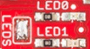
As mentioned on the previous page, LEDs 0 and 1 provide some easily accessible feedback on the current state of the module. Here's a decoder ring for sorting out what they mean.
| LED 0 Blue |
LED 1 Red |
Status |
|---|---|---|
| BLINK | OFF | Scanning |
| OFF | BLINK | Advertising |
| ON | OFF | Connected Central |
| OFF | ON | Connect Peripheral |
| ON | ON | Idle |
Note: the LEDs will change to represent the current settings of the module when changing into scanning, advertising, or idle modes, but the module will not change state until the changes have been written to non-volatile memory and the module has been rebooted.
LEDS Jumper
This jumper disconnects the cathode side of the LEDs from the ground plane, disabling them and eliminating the few hundred microamps each one draws under normal circumstances. It ships closed by default.
INP and REG Jumpers

The INP jumper, pictured above, has four possible configurations but only three valid ones.
This is the default mode, as it ships. In this mode, the input voltage from the VCC pin on the 6-pin header and the VIN pin on the GPIO header is routed to the 3.3V regulator.

In this mode, the input side of the regulator is disconnected from all pins, and the module's supply is connected directly to the VIN pin and the VCC pin. In this situation, the voltage present on the input must be between 1.8V and 4.3V. That's within the range of a single-cell LiPo battery, but not of a 5V target board!
It's probably a good idea to clear the REG jumper at this point, too; putting a voltage on the output of the regulator but not on the input is liable to cause odd behavior.
The level shifting circuit is still active here, so if the data lines on your processor are at a higher voltage than the BC118 is being fed, communications will still work.

With no solder on the jumper, you've completely disconnected the module from the VCC and VIN pins entirely. You'll need to provide power to the 3.3V pin on the GPIO header directly, with the same caveat as earlier regarding the voltage range.
Again, you should clear the REG jumper.
Finally, the fourth mode, which I'm not only going to include a picture of, it's so inappropriate: a big old solder glob covering all three pads. Don't do this. Seriously. It probably won't do anything bad, but it's not going to help your current consumption any, it may damage the regulator, and it will bypass the regulator. Just don't do it.