TSH82 Configurable OpAmp Hookup Guide
Introduction
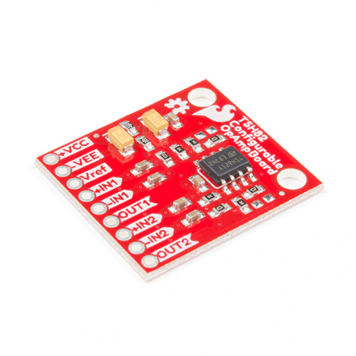
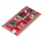
The TSH82 Configurable OpAmp board was designed to give you the best combination of performance and flexibility that we could achieve. The TSH82 device itself has 2 gain stages, each one independently accessible via header. Each stage is natively configured as an inverting amplifier, giving you a gain of -4.7 with AC input coupling. Stringing both stages together gives you a gain of about 22. But with the use of the jumpers on the back of the board, you can additionally configure each stage for non-inverting operation, differential input, and DC input coupling. The board will also operate with a single-ended DC power supply of 4.5V to 12V, or a bipolar supply from +/-2.25V to +/-6V.
Required Materials
In order to get signals in and out of the board, you're going to have to solder some stuff together. You may not need everything on this list, depending on what you have. Add it to your cart, read through the guide, and adjust the cart as necessary.
Suggested materials
In order to tailor the board to your specifications, you might want some other parts that we can offer.
You may also want to examine these signals in real time as you're working with them, or maybe generate a signal to run through your opamp board.
Digital Storage Oscilloscope - 100MHz (TBS2104)
TOL-14925Suggested Reading
If any of this is new to you, have a look through these - the OpAmp intro with LT Spice is particularly good as an opamp primer.
How to Solder: Through-Hole Soldering
How to Use an Oscilloscope
Introduction to Operational Amplifiers with LTSpice
Hardware Overview
The TSH82 Configurable OpAmp Board is meant to be hacked on, so you'll want to be familiar with the sections of the circuitry.
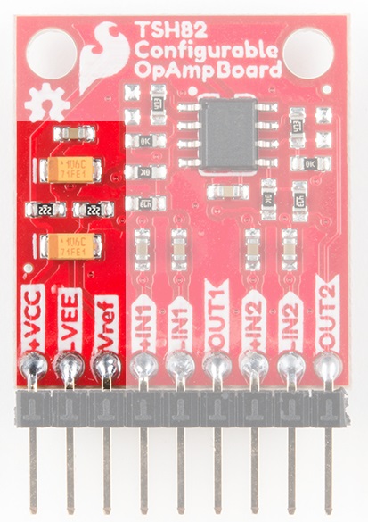
On the far left side of the board is the power and reference section, the middle section covers stage 1 of the amplifier, and the far right side has stage 2. Each section also has three corresponding pins directly below in the picture.
Power and Reference
Positive voltage goes into +VCC, and negative voltage (or ground) goes into -VEE. The board generates an onboard reference voltage by way of two 2.2k 1% resistors decoupled with 10.1uF, giving a value halfway between +VCC and -VEE with a low frequency cutoff of about 15Hz. If you need better performance, VREF is accessible from the header and can be driven to any voltage between +VCC and -VEE without damaging the board.
Stages One and Two
Electrically speaking, the stages are identical. The default configuration is inverting with a gain of -4.7 with a bandwidth of almost 10MHz. Signal input is on -IN1 and output is taken from OUT1 (or -IN2 and OUT2 for stage two). Input signals are AC coupled with 1.0uF caps, and the input impedance is 10K with a low frequency cutoff of 15.9Hz. Outputs are DC coupled, so don't forget to add a capacitor to the output if you're running a single-ended supply and need to strip out the DC component. Of course, this isn't an issue if you're running the output of stage 1 to the input of stage 2.
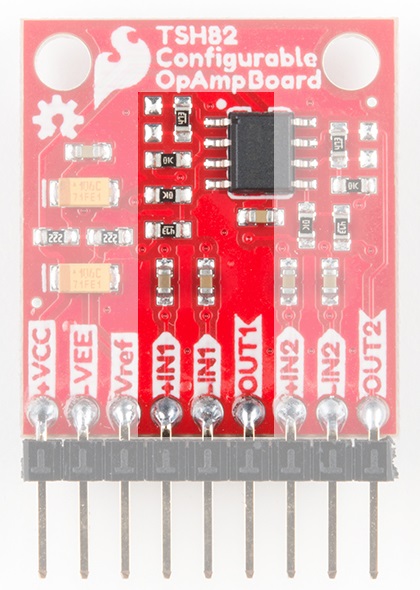 |
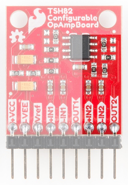 |
| Stage 1 | Stage 2 |
All Those Jumpers
On the back of the board you'll find 10 solder jumpers that can be used to change the board's performance, but nothing there needs to be changed to use it in it's default state. To demonstrate how to use the jumpers, we'll first describe their functions, then show you different circuit configurations with corresponding jumper settings. For the sake of clarity, it might be a good idea to have the schematic open for reference as you read through the jumper settings description.
Stage 1:
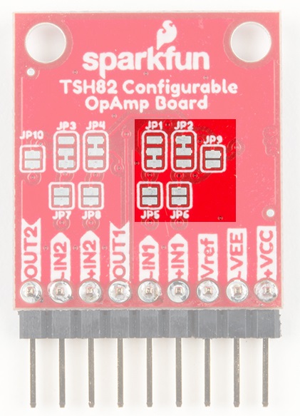 |
 |
| Stage 1 | Stage 1 Schematic |
Stage 2:
 |
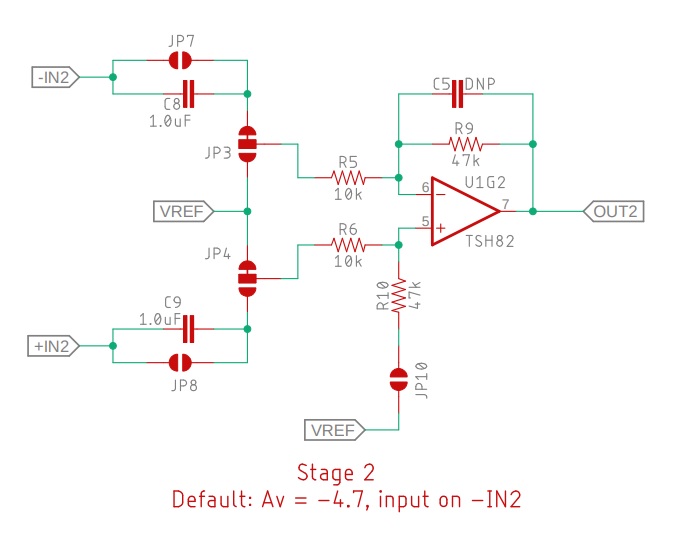 |
| Stage 2 | Stage 2 Schematic |
Input signal path:
- JP1 and JP2 - 3 way solder jumpers used to change the input signal path in Stage 1.
- JP1 - inverting input
- JP2 - non-inverting input
- JP3 and JP4 - 3 way solder jumpers used to change the input signal path in Stage 2.
- JP3 - inverting input
- JP4 - non-inverting input
There are small traces within these jumpers to set the default inverting configuration that will have to be cut out if you wish to change to differential or non-inverting configurations.
AC vs DC coupling
- JP5 and JP6 - Solder jumper used to select between AC and DC coupling for the inputs to Stage 1.
- JP5 - inverting input
- JP6 - non-inverting input
- JP7 and JP8 - Solder jumper used to select between AC and DC coupling for the inputs to Stage 2.
- JP7 - inverting input
- JP8 - non-inverting input
Vref
- JP9 - allows the user to tie the non-inverting input of stage 1 to Vref through a 47k resistor for differential operations.
- JP10 - same functionality as JP9 but for stage 2
As you can see, there are a lot of options. But if any of that leaves you confused, let us show you some workable configurations!
Configurations
Inverting, Gain = -4.7, AC-coupled Input, 0-10V Supply (Default)
This is the easiest configuration to use as it requires no changes to the jumpers on the board.
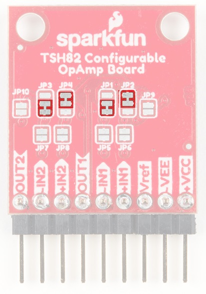
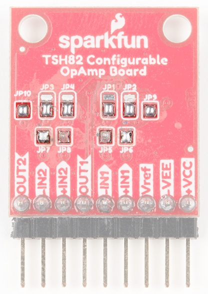
In the picture below, the jumper settings for this default mode are highlighted for your reference. Note the small traces bridging the pads of the solder jumpers. If the board does not perform as expected, double check that these traces are still present. If they're not, just replace them with a blob of solder to make the default connections as shown here.
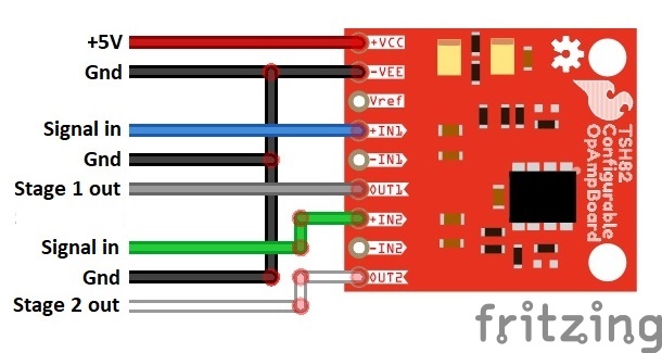
+10VDC power input is on +VCC and ground is on -VEE. Vref will assume a value near +5V.
For stage 1, signal input is between -IN1 and -VEE, and output is taken between OUT1 and -VEE. It's effectively the same for stage 2: signal input is between -IN2 and -VEE, and output is taken between OUT2 and -VEE. Each stage will give you a gain of -4.7, so to keep the output in the linear region your input signal can't be more than 2.12Vpp, as calculated here:
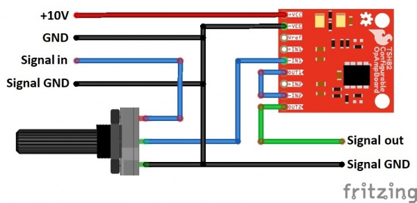
If you're running both stages in sequence, that maximum becomes 453mVpp. If you're not sure what your input signal magnitude is going to be, it's probably a good idea to use a potentiometer at the input of your circuit.
Differential Input, Gain = 4.7, DC-coupled Input, 0-5V Supply
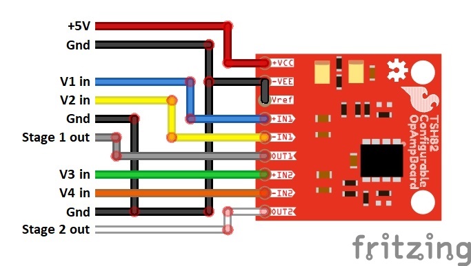
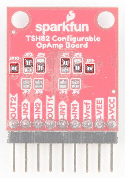
Differential configuration gives the user the ability to compare two dynamic voltages rather than comparing one against a static reference. The jumper settings for differential configuration are as shown below.
The picture above shows both stages set up for differential operation with DC input coupling (jumpers 5-8 are set). Put your first signal input, V1, between +IN1 and ground, and put your second signal input, V2, between -IN1 and ground. +5V goes in on +VCC and ground goes to -VEE. Also, set Vref to 0V by connecting the Vref header pin to -VEE. Gain for the circuit is 4.7, as calculated here:
And, of course, all of this also applies to stage 2, just transpose all the numbers in the pin names from 1's to 2's.
Non-inverting, Gain = 4.7, AC-coupled Input, 0-6V Supply
While the classic non-inverting topology can’t be realized without replacing parts on the board, non-inverting functionality can be achieved by starting with the differential configuration and tying the inverting input to Vref. The jumper settings can be seen below.
The circuit is fully functional, but it's got a couple of quirks that the user should be aware of before use. First, because this isn't the "normal" non-inverting circuit topology, gain is about 4.7 instead of 5.7. Second, and for the same reason, there's some input offset that you might have to deal with, but it's not complicated. Specifically with this topology, Vref will normally sit halfway between +VCC (6V) and -VEE (0V), but the output will skew somewhat positive, to around 4V without any signal input. As a result, your output swing can only go +/-2V around Vref before it starts to clip, making your maximum allowable input signal about 851mVpp. If those numbers work for your design, then you're good to go!
On the other hand, if you move Vref (covered in the next section) to about 1.6V, the output will come back to 3V and allow the full +/-3V output swing. Dividing by our gain of 4.7 gives us a maximum input signal of 1.28Vpp, which is still less than the 3.6Vpp allowable window created by moving the reference voltage.
Hacking the Board
Changing Gain or Bandwidth
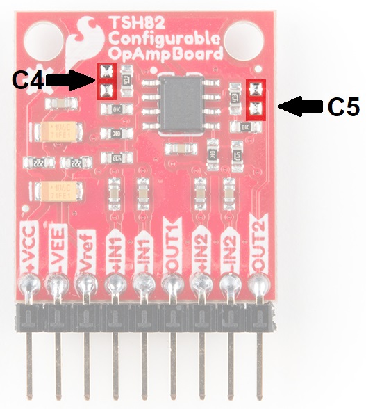
By this time, you’ve probably asked yourself about those two missing components. “What’s up with that? Did I get a bum board?” Nope, those footprints are intentionally left open for you to change the circuit behavior. Primarily, we’re talking about augmentations of the inverting configuration, as achieving similar results otherwise would require replacing parts; do-able, but more work and probably not necessary.
In the schematic, the parts are shown as C4 for stage one (on the left) and C5 for stage 2 (on the right).
There are two easy things you can change about the circuits’ behavior using the C4 and C5 footprints. First, you can alter it’s high frequency cutoff by adding a capacitor, as calculated from
where f is the desired cutoff frequency, and C is capacitance in farads. If you’re working with lower-frequency signals and you’re concerned about high-frequency noise, this is an addition you might consider.
The second thing you can do is to reduce the gain in order to increase the bandwidth by placing a resistor instead of a cap. Gain is calculated from
where R is the new component. For example, if you place an additional 47k resistor it will reduce your gain by half (Av = 2.35), but it will increase your workable bandwidth to around 18MHz.
Dialing In your Reference
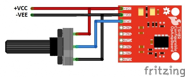
As described in the section on non-inverting functionality, you may have reason to move your reference voltage (Vref) around. The easiest way to do this is with a potentiometer with one end on -VEE, another on +VCC and the wiper on Vref (10k is a good choice). This puts the potentiometer in parallel with the 2.2k resistor divider that sets Vref natively and allows you to set the reference to any value easily.
The on-board reference voltage is heavily decoupled with tantalum and ceramic capacitors to keep noise low. But if you need it lower, you might consider using a dedicated voltage source as the reference instead of the 2.2k resistor divider provided. Just attach your source to -VEE (0V) and Vref (positive voltage).
Resources and Going Further
For more information, check out the resources below:
We’ve tried to pack as much functionality and flexibility into the TSH82 Configurable OpAmp Board as possible, but at some point the compromises become crippling. That said, if you’re adept with a soldering iron, this board can be the foundation of many other topologies - from RF signals to audio to testing scenarios. Check out some of the following if you need inspiration for your next project:
Also - check out Music From Outer Space (MFOS). The website offers hundreds of schematics to help you get into DIY Synths and creator Ray Wilson made this MFOS Virtual Operational Amplifier Application, which allows us to experiment with op amps while viewing the output on a simulated oscilloscope.
Have you augmented yours? Leave us a comment and maybe we’ll add it to the tutorial!
