Qwiic Dynamic NFC/RFID Tag Hookup Guide
 El Duderino
Hardware Overview
Let's take a closer look at the ST25DV64KC and other hardware present on the Qwiic Dynamic NFC/RFID Tag.
ST25DV64KC Dynamic NFC/RFID Tag
The ST25DV64KC from STMicroelectronics is a unique tag IC that communicates over both I2C and RF (NFC). It conforms to ISO/IEC 15693 (13.56 MHz frequency) and NFC Forum Type 5 recommendations.
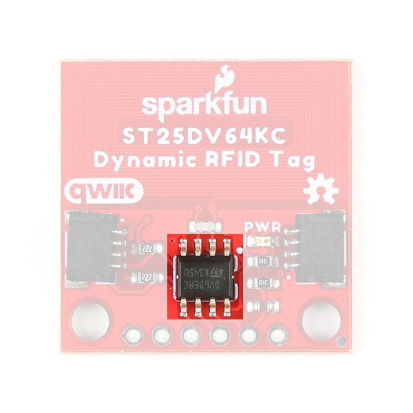
The ST25DV64KC includes 64 Kbit EEPROM for users to write and read data from, a general purpose output to act as an external interrupt reporting events such as RF field changes, RF activity, I2C writes and RF switch toggling over I2C. The IC has a supply voltage range of 1.8V to 5.5V though when in a Qwiic circuit it runs at 3.3V. It also includes an energy harvesting pin capable of outputing µW of power with an RF field of sufficient strength. For a complete overview of the ST25DV64KC, refer to the datasheet.
The ST25DV64KC supports a fast transfer mode to send the contents of a 256 byte buffer between a device connected to the tag over I2C (refered to as the tag's Mailbox) and an RF device such as a reader or smartphone. This makes it so you can store data on the tag and have it available for reading by an RF device by simply bringing it into the RF read range, even if the tag is powered off. This data can also be password protected with a 64-bit value.
Power and Communication Interfaces
The Qwiic Dynamic NFC/RFID Tag has two interfaces for powering and communicating with the ST25DV64KC: a pair of Qwiic connectors and a plated through hole (PTH) header.
Qwiic Connector
The board has a pair of Qwiic connectors to integrate it into a Qwiic ecosystem.
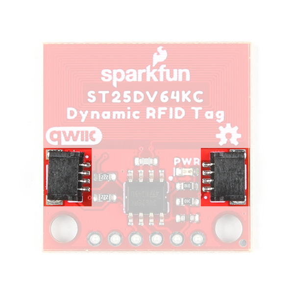
The Qwiic connectors route the SDA/SCL connections as well as 3.3V and Ground to power the board and communicate with the ST25DV64KC over I2C.
Plated Through Hole Header
The board has a 0.1"-spaced PTH header that breaks out the power pins (3.3V and Ground), I2C interface (SDA/SCL), energy harvesting pin (VEH), and general purpose output pin (GPO).

The Energy Harvesting Pin outputs an analog voltage when energy harvesting mode is enabled and in the presence of a strong enough RF field. Refer to section 5.5 of the datasheet for specifics on using this pin. The General Purpose Output is an open-drain configurable pin used for interrupt events.
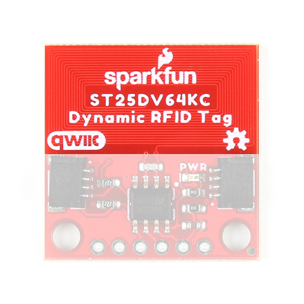
Antenna
The board includes a PCB antenna for the ST25DV64KC to help boost the read range a bit. In our testing with a smart phone running an NFC reader app we found it had a range of a few centimeters.
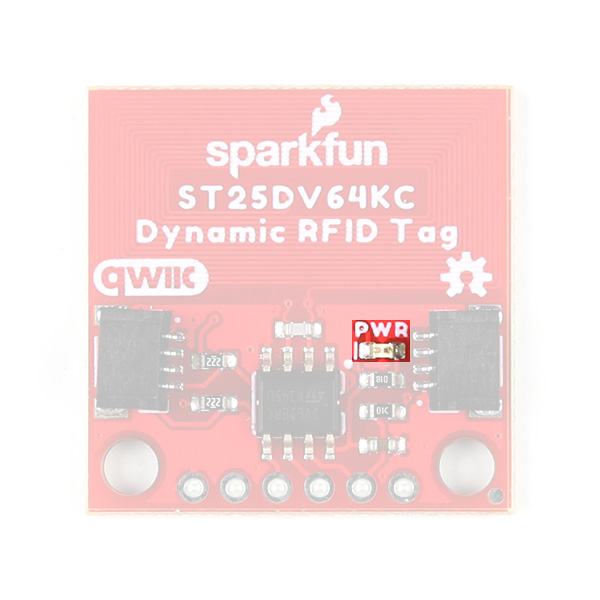
LED
The sole LED on this board is a power status LED.
Solder Jumpers
The board has three solder jumpers labeled LED, GPO and I2C. The table below outlines their labels, default state, functionality, and any notes regarding their use.
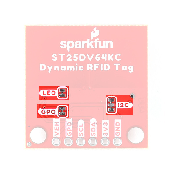
| Label | Default State | Function | Notes |
|---|---|---|---|
| LED | CLOSED | Completes the Power LED circuit. | Open to disable the Power LED. |
| GPO | CLOSED | Pulls the interrupt (GPO) pin HIGH through a 10kΩ resistor. | Open to disable the pullup resistor. |
| I2C | CLOSED | Pulls the SDA/SCL lines to VCC (3.3V) through a pair of 2.2kΩ resistors. | Open to disable the pullup resistors. |
Board Dimensions
The Qwiic Dynamic NFC/RFID Tag matches the standard Qwiic breakout size of 1" x 1" (25.4mm x 25.4mm) and has two mounting holes that fit a 4-40 screw.
