PCB Basics
Contributors:
 SFUptownMaker
SFUptownMaker 
Terminology
Now that you've got an idea of what a PCB structure is, let's define some terms that you may hear when dealing with PCBs:
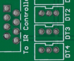
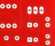
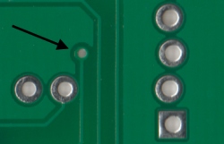
- Annular ring - the ring of copper around a plated through hole in a PCB.
Examples of annular rings.
- DRC - design rule check. A software check of your design to make sure the design does not contain errors such as traces that incorrectly touch, traces too skinny, or drill holes that are too small.
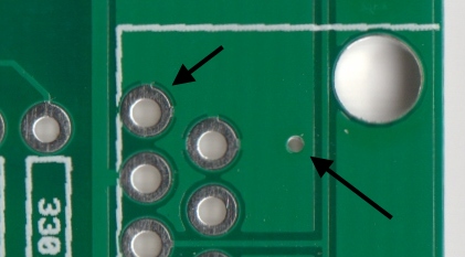
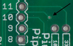
- Drill hit - places on a design where a hole should be drilled, or where they actually were drilled on the board. Inaccurate drill hits caused by dull bits are a common manufacturing issue.
Not so accurate, but functional drill hits.
- Finger - exposed metal pads along the edge of a board, used to create a connection between two circuit boards. Common examples are along the edges of computer expansion or memory boards and older cartridge-based video games.
- Mouse bites - an alternative to v-score for separating boards from panels. A number of drill hits are clustered close together, creating a weak spot where the board can be broken easily after the fact. See the SparkFun Protosnap boards for a good example.
Mouse bites on the LilyPad ProtoSnap allow the PCB to be snapped apart easily.
Note: Looking for more information about mousebites and how to integrate it in your designs? Try checking out the blog post below!
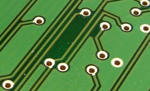
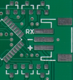
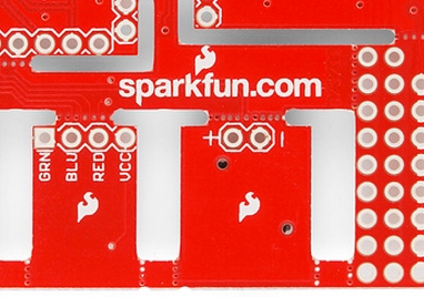
- Pad - a portion of exposed metal on the surface of a board to which a component is soldered.
PTH (plated through-hole) pads on the left, SMD (surface mount device) pads on the right.
- Panel - a larger circuit board composed of many smaller boards which will be broken apart before use. Automated circuit board handling equipment frequently has trouble with smaller boards, and by aggregating several boards together at once, the process can be sped up significantly.
- Paste stencil - a thin, metal (or sometimes plastic) stencil which lies over the board, allowing solder paste to be deposited in specific areas during assembly.
Abe does a quick demonstration of how to line up a paste stencil and apply solder paste.
- Pick-and-place - the machine or process by which components are placed on a circuit board.
Bob shows us the SparkFun MyData Pick and Place machine. It's pretty awesome.
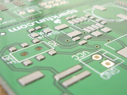
- Plane - a continuous block of copper on a circuit board, define by borders rather than by a path. Also commonly called a "pour".
Various portions of the PCB that have no traces but has a ground pour instead.
- Plated through hole - a hole on a board which has an annular ring and which is plated all the way through the board. May be a connection point for a through hole component, a via to pass a signal through, or a mounting hole.
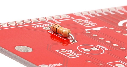
A PTH resistor inserted into the FabFM PCB, ready to be soldered. The legs of the resistor go through the holes. The plated holes can have traces connected to them on the front of the PCB and the rear of the PCB.
- Pogo pin - spring-loaded contact used to make a temporary connection for test or programming purposes.
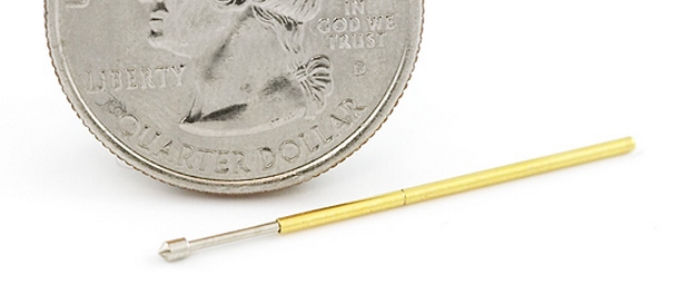
The popular pogo pin with pointed tip. We use tons of these on our test beds.
- Reflow - melting the solder to create joints between pads and component leads.
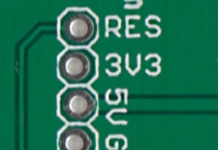
- Silkscreen - the letters, number, symbols, and imagery on a circuit board. Usually only one color is available, and resolution is usually fairly low.
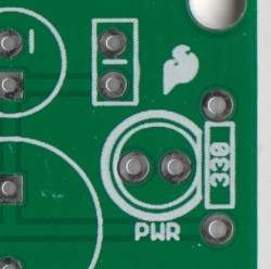
Silkscreen identifying this LED as the power LED.
- Slot - any hole in a board which is not round. Slots may or may not be plated. Slots sometimes add to add cost to the board because they require extra cut-out time.
Complex slots cut into the ProtoSnap - Pro Mini. There are also many mouse bites shown. Note: the corners of the slots cannot be made completely square because they are cut with a circular routing bit.
- Solder paste - small balls of solder suspended in a gel medium which, with the aid of a paste stencil, are applied to the surface mount pads on a PCB before the components are placed. During reflow, the solder in the paste melts, creating electrical and mechanical joints between the pads and the component.
Solder paste on a PCB shortly before the components are placed. Be sure to read about *paste stencil above as well.*
- Solder pot - a pot used to quickly hand solder boards with through hole components. Usually contains a small amount of molten solder into which the board is quickly dipped, leaving solder joints on all exposed pads.
- Soldermask - a layer of protective material laid over the metal to prevent short circuits, corrosion, and other problems. Frequently green, although other colors (SparkFun red, Arduino blue, or Apple black) are possible. Occasionally referred to as "resist".
Solder mask covers up the signal traces but leaves the pads to solder to.
- Solder jumper - a small, blob of solder connecting two adjacent pins on a component on a circuit board. Depending on the design, a solder jumper can be used to connect two pads or pins together. It can also cause unwanted shorts.
- Surface mount - construction method which allows components to be simply set on a board, not requiring that leads pass through holes in the board. This is the dominant method of assembly in use today, and allows boards to be populated quickly and easily.
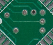
- Thermal - a small trace used to connect a pad to a plane. If a pad is not thermally relieved, it becomes difficult to get the pad to a high enough temperature to create a good solder joint. An improperly thermally relieved pad will feel "sticky" when you attempt to solder to it, and will take an abnormally long time to reflow.
On the left, a solder pad with two small traces (thermals) connecting the pin to the ground plane. On the right, a via with no thermals connecting it completely to the ground plane.
- Thieving - hatching, gridlines, or dots of copper left in areas of a board where no plane or traces exist. Reduces difficulty of etching because less time in the bath is required to remove unneeded copper.
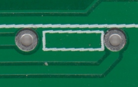
- Trace - a continuous path of copper on a circuit board.
-> A small trace connecting the Reset pad to elsewhere on the board. A larger, thicker trace connects to the 5V power pin. <-
- V-score- a partial cut through a board, allowing the board to be easily snapped along a line.
- Via - a hole in a board used to pass a signal from one layer to another. Tented vias are covered by soldermask to protect them from being soldered to. Vias where connectors and components are to be attached are often untented (uncovered) so that they can be easily soldered.
Front and back of the same PCB showing a tented via. This via brings the signal from the front side of the PCB, through the middle of the board, to the back side.
- Wave solder - a method of soldering used on boards with through-hole components where the board is passed over a standing wave of molten solder, which adheres to exposed pads and component leads.