MiniGen Hookup Guide
 SFUptownMaker
Connections
Top
Here's the top of the board. Due to the tight layout and lack of space on this shield, the labels had to live on the bottom side of the PCB.

There are two output sources: a 2x1 0.1" spaced header and a u.FL connector. The u.FL connector is shield as ground.
The output end of the board should be at the opposite end from the FTDI connector when installed on a Pro Mini.
Bottom
Take a look at the picture above. Let's go through the labeled connections one at a time.
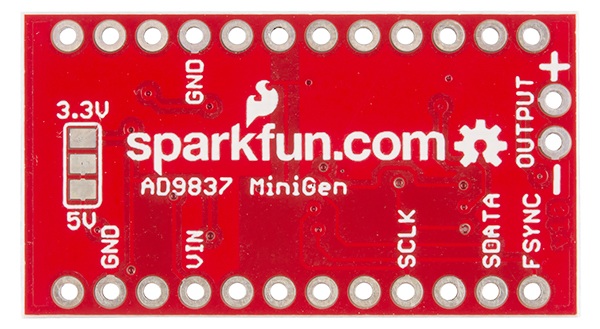
- GND - Only one of these needs to be connected at a time; that means you can get away with headers on one side only.
VIN - By default, this goes to a 3.3V regulator. If you want to use the board with a 5V Pro Mini, you should put a blob of solder on the jumper pads on the back to connect all three together.
Danger! Adding a solder jumper will bypass the 3.3V voltage regulator, you will be powering the board at 5V. While most of the components on the board can handle 5V, the 16MHz crystal oscillator is not. It can only handle 3.3V. You would need to find a way to cut the trace connecting to the 16MHz and 3.3V voltage regulator in order to reroute 3.3V to the 16MHz crystal oscillator's circuit.- OUTPUT+ - This is the anti-aliased output from the AD9837. Expect to see a 1Vp-p signal, offset from ground by 1/2 Vin.
- OUTPUT- - Connected to ground.
- SCLK - SPI clock input. The SPI bus can handle up to 40MHz input.
- SDATA - Input from the master device. Note that register contents cannot be read out from the AD9837 part; it lacks a DOUT pin.
- FSYNC - Equivalent to chip select.
SPI interface
As mentioned above, the SPI interface can be driven at up to 40MHz. The SPI interface should be at or close to the supply voltage for the chip (3.3V by default).
If you elect to write your own SPI control for this, the clock idles low (CPOL = 0), and data is latched on the rising edge (CPHA = 1). This corresponds to SPI Mode 2.