MicroMod Machine Learning Carrier Board Hookup Guide
 Nate, Ell C
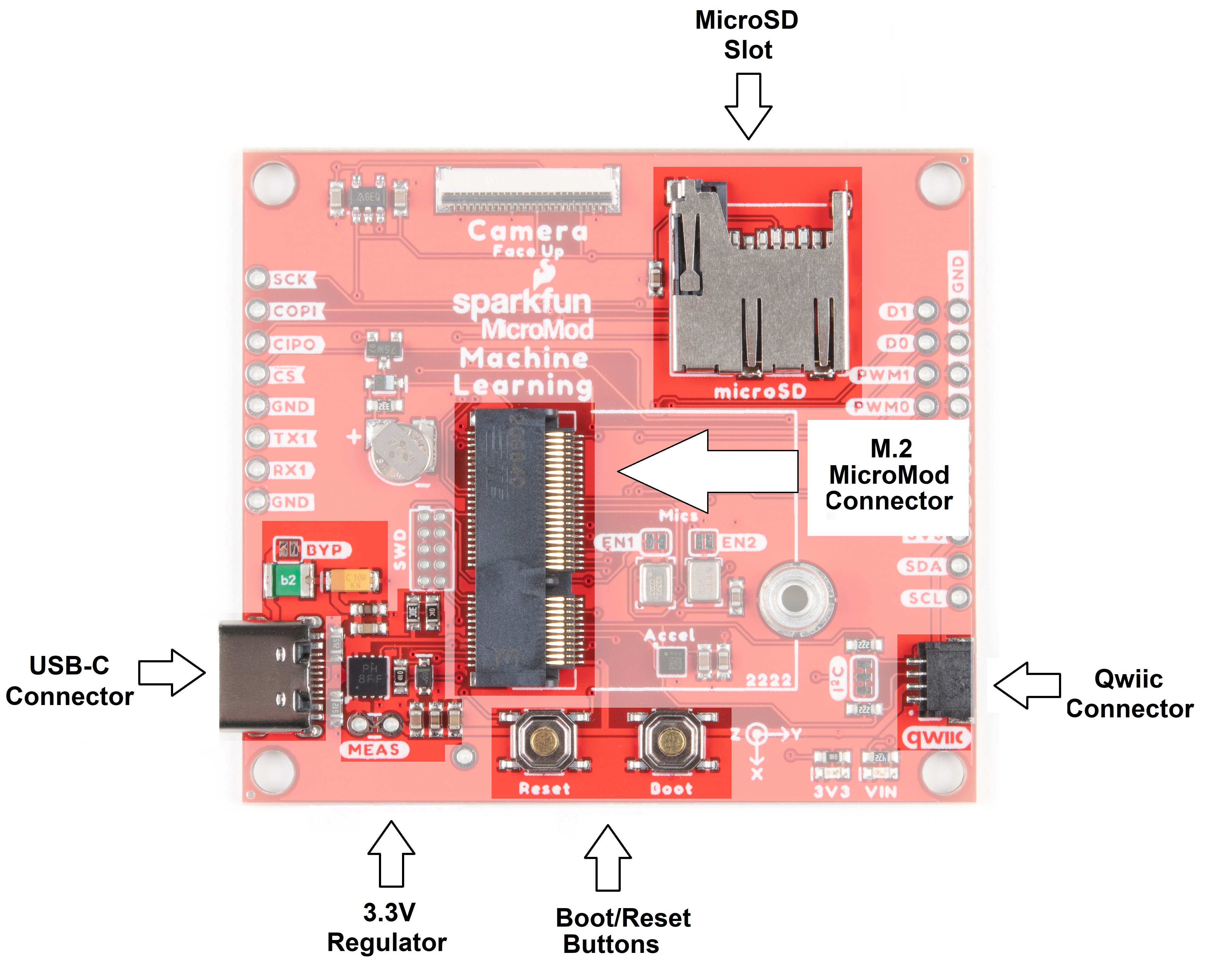
Hardware Overview
Common Components
Most SparkFun MicroMod Carriers will have some common components and all MicroMod Carriers will have the keyed M.2 MicroMod Connector to plug your processor into. The photo and list below outline some of the components you can expect on most SparkFun MicroMod Carriers.
- M.2 MicroMod Connector - This special keyed M.2 connector lets you install your MicroMod Processor of choice on your Machine Learning Carrier Board.
- USB-C Connector - Connect to your computer to program your Processor and also can provide power to your MicroMod system.
- 3.3V Regulator - Provides a regulated 3.3V and sources up to 1A.
- Qwiic Connector - The standard Qwiic connector so you can add other Qwiic devices to your MicroMod system.
- Boot/Reset Buttons - Push buttons to enter Boot Mode on Processor boards and to Reset your MicroMod circuit.
- microSD Slot - Insert a microSD card for reading and writing data.
Machine Learning MicroMod Carrier Board Specific Components
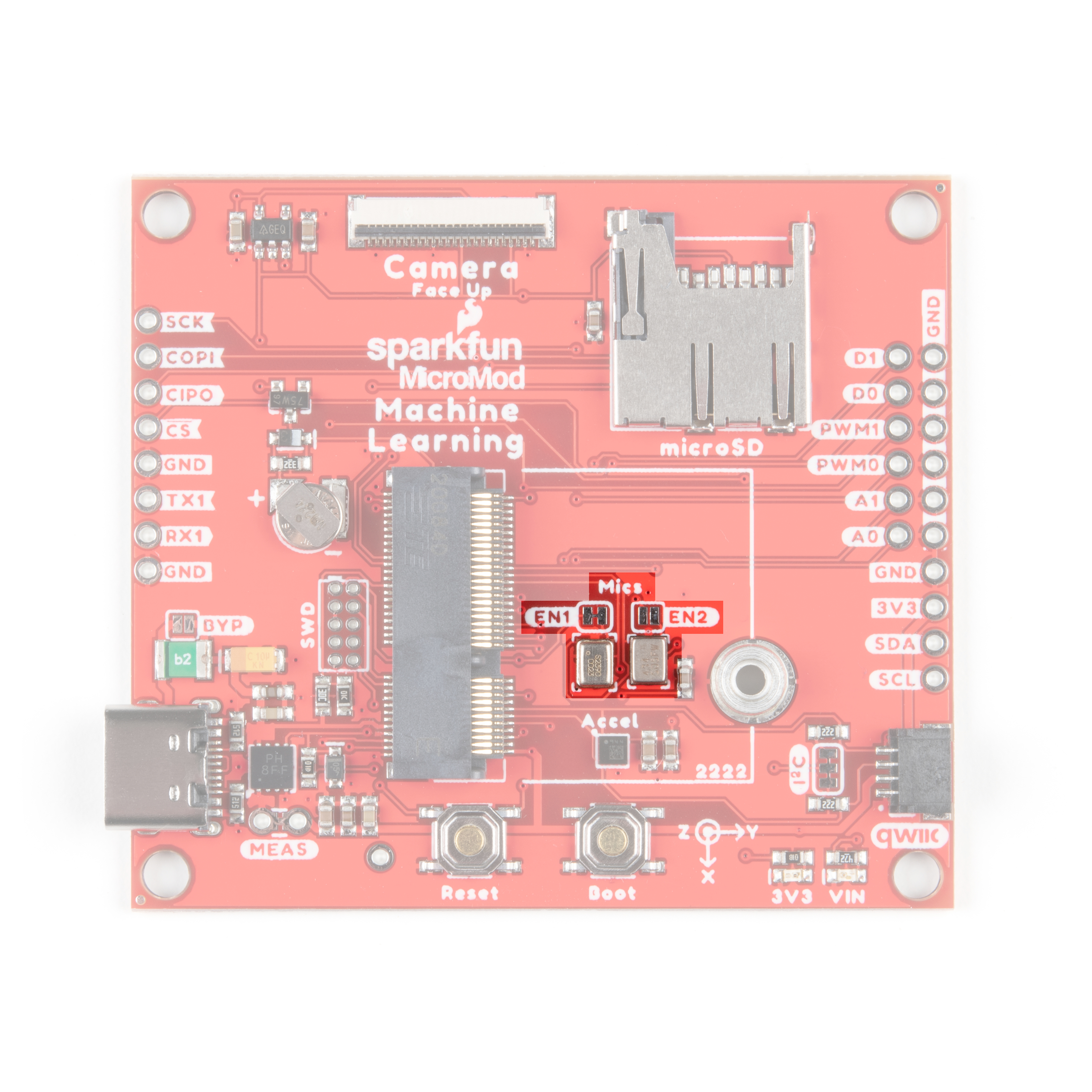
Digital MEMS Microphones
What's better than ONE microphone? TWO!
- Microphone 1 supports a PDM interface and is enabled by default. To disable this mic, cut the EN1 jumper. For more information on this microphone, refer to the datasheet here.
- Microphone 2 supports an I2S interface and is disabled by default. To enable EN2, solder the jumper pads to close the circuit. For more information on this microphone, refer to the datasheet here.
GPIO
Along the sides of the Machine Learning Carrier Board, we've broken out dedicated PTHs for UART, digital, analog, pulse width modulation, and SPI. You may also notice that we've included a ground rail on the right side of the board.
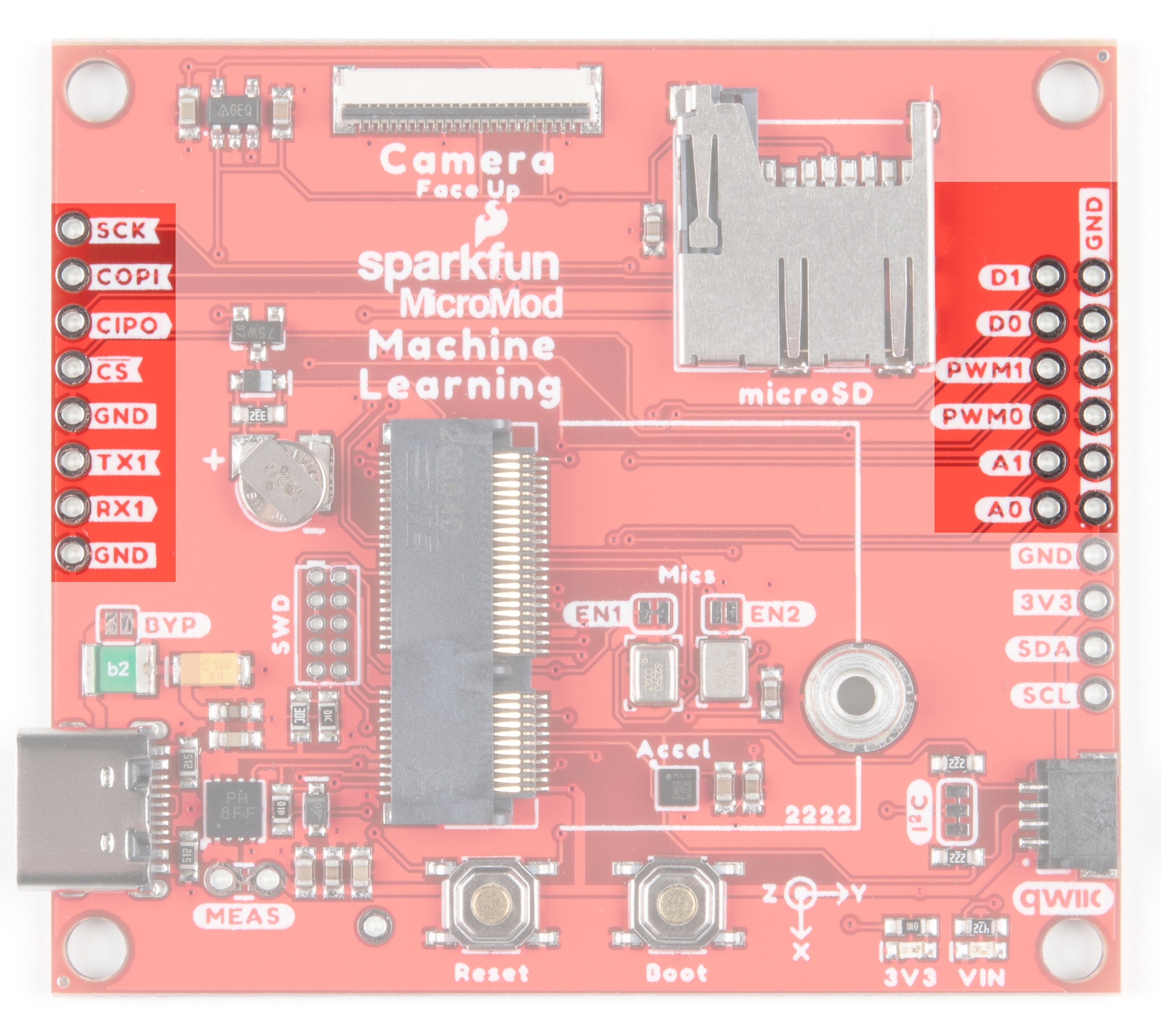
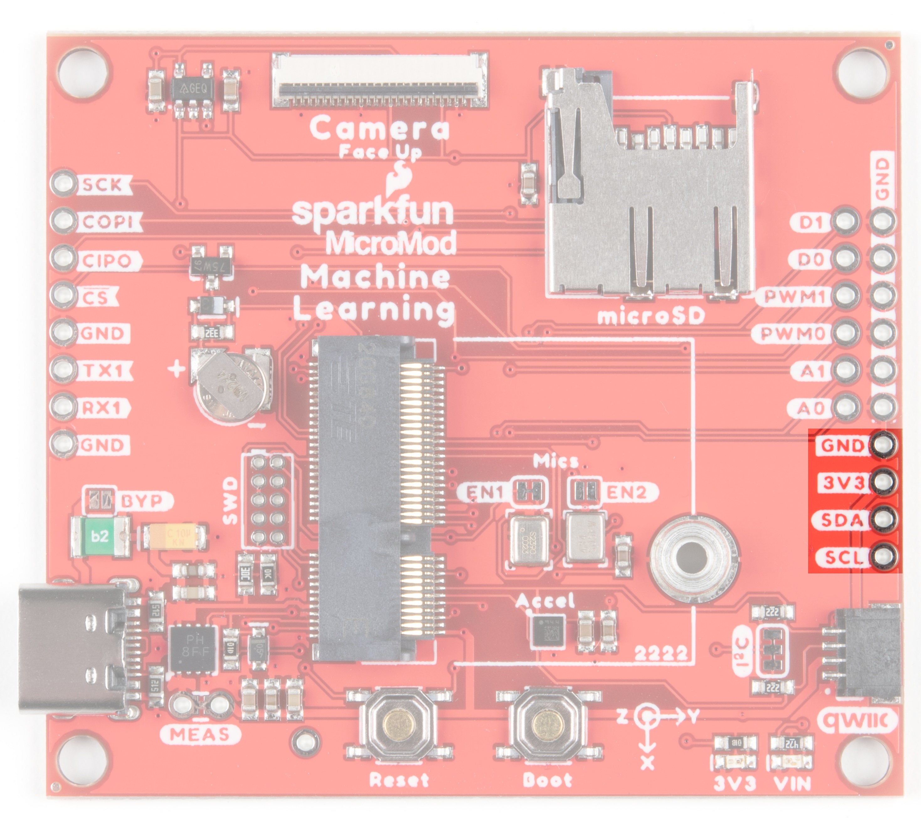
I2C Specific GPIO
Additionally, we've broken out the I2C SDA and SCL lines, with 3V3 and GND to complete your I2C functionality. These are primary I2C pins - they are connected to the Qwiic connector.
Accelerometer
The LIS2DH12 is an ultra-low-power, high performance, three-axis linear accelerometer belonging to the “femto” family with digital I2C/SPI serial interface standard output. If you need more detail on this little guy, refer to the Datasheet here.
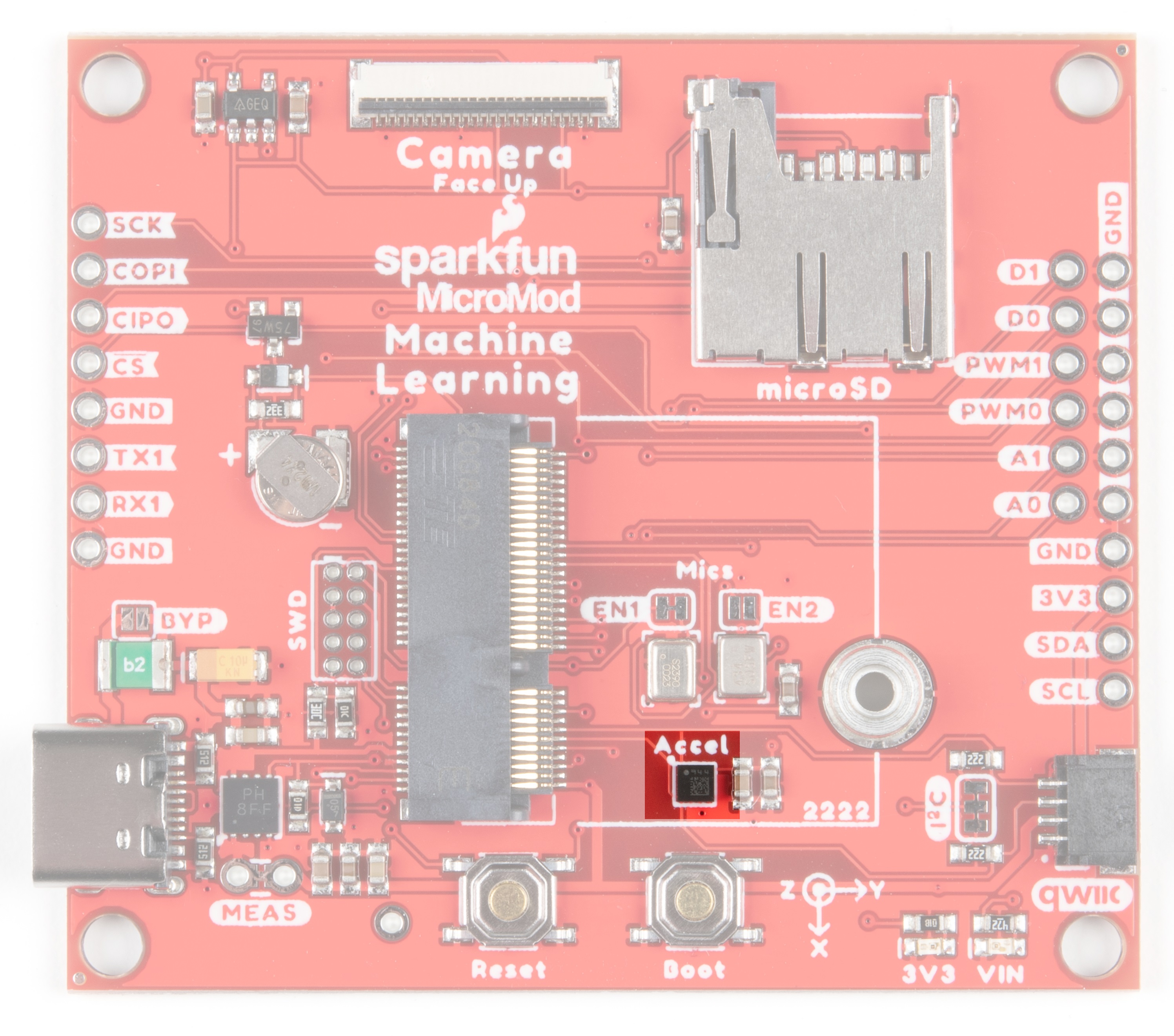
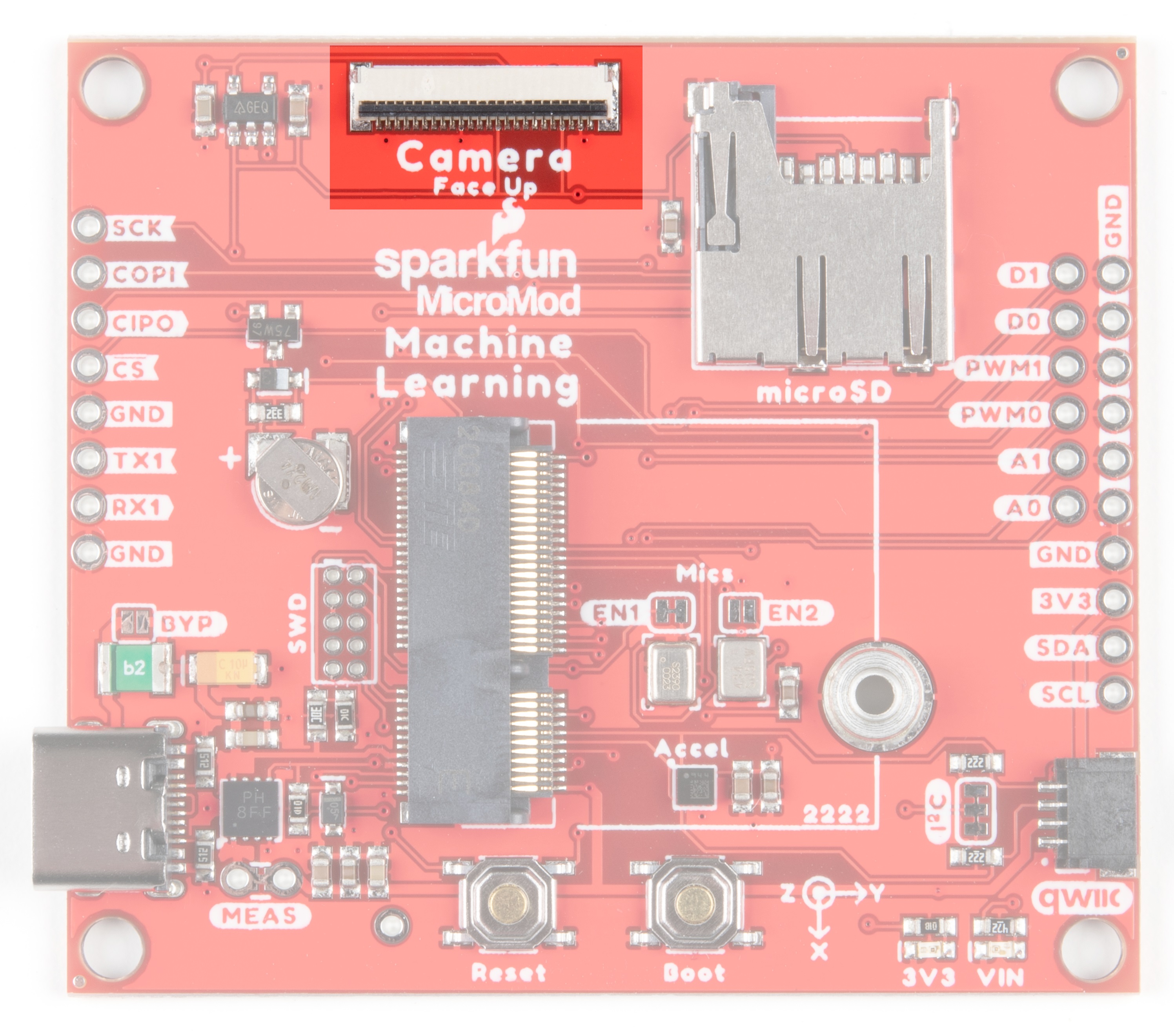
Camera Connector
With this 24 pin connector, you can add image recognition to your machine learning board by popping in the Himax CMOS Imaging Camera.
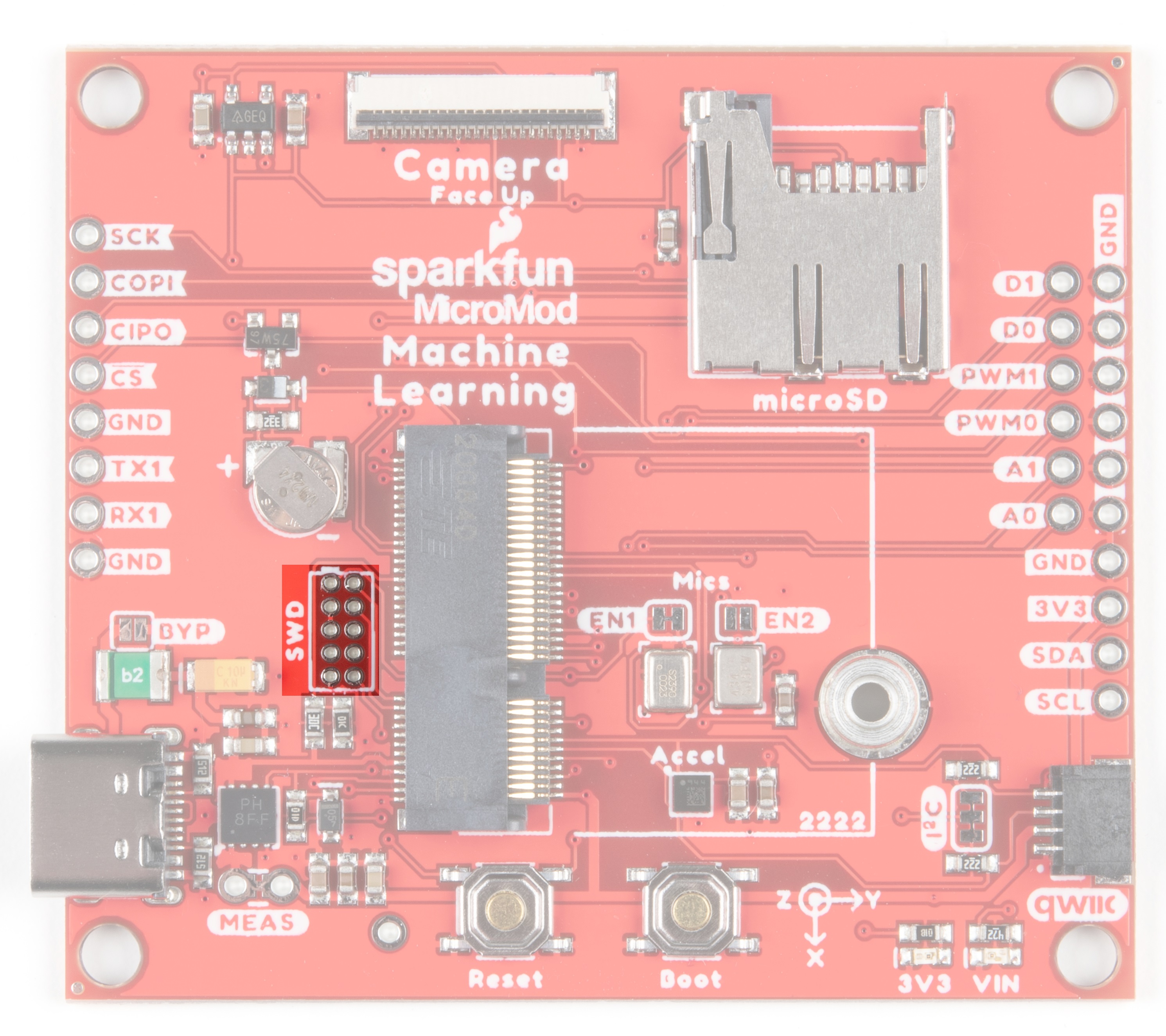
JTAG
An unpopulated JTAG footprint is available for more advanced users who need breakpoint level debugging. We recommend checking out our JTAG section for the compatible male header and a compatible JTAG programmer and debugger.
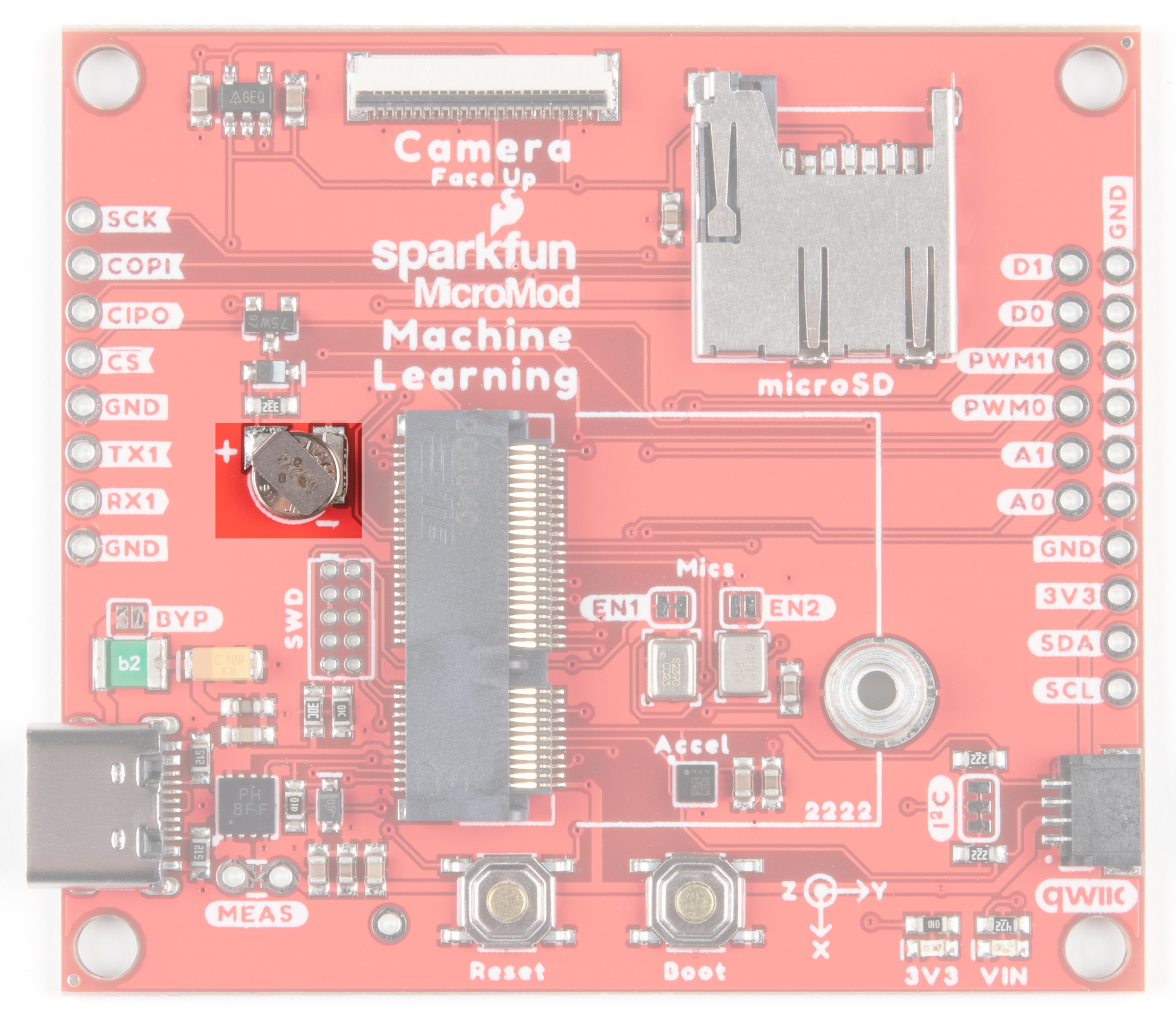
RTC Battery
We've included a 3V Lithium Rechargeable Battery as a backup power source.
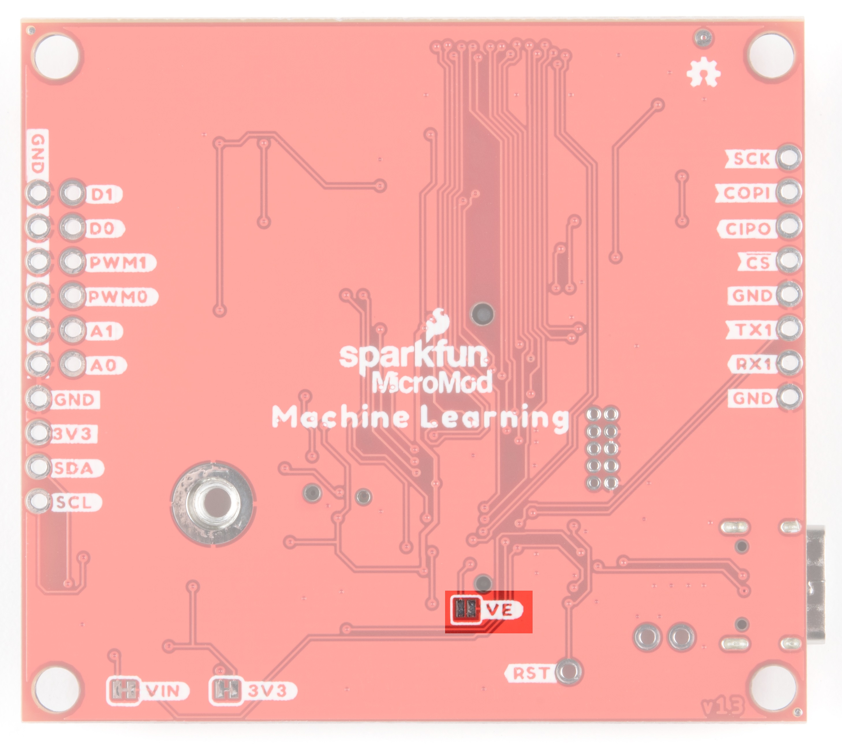
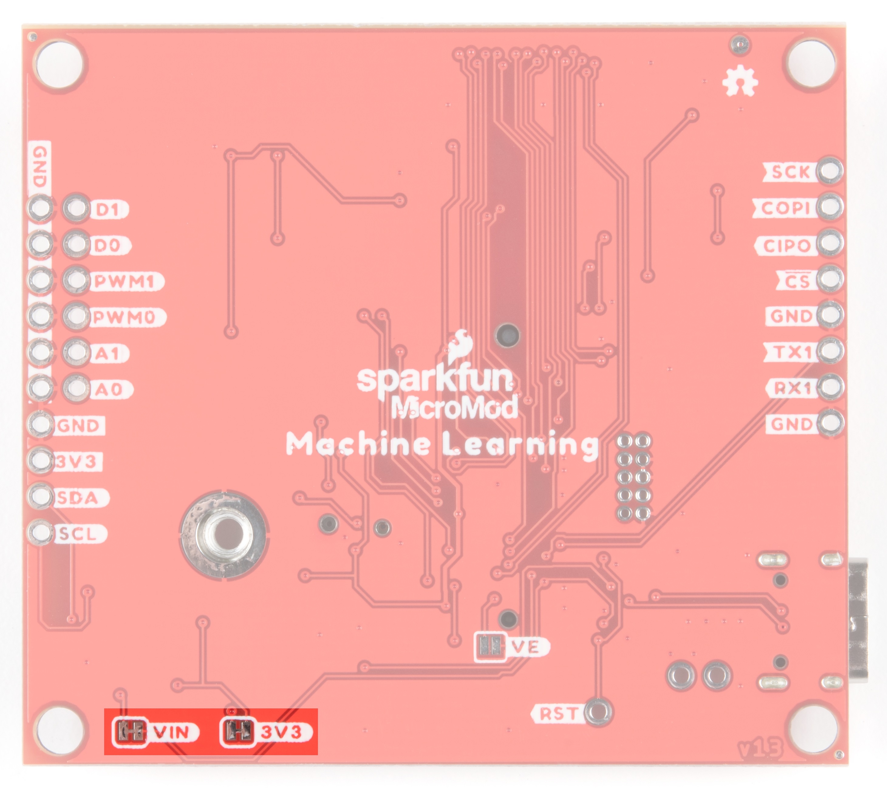
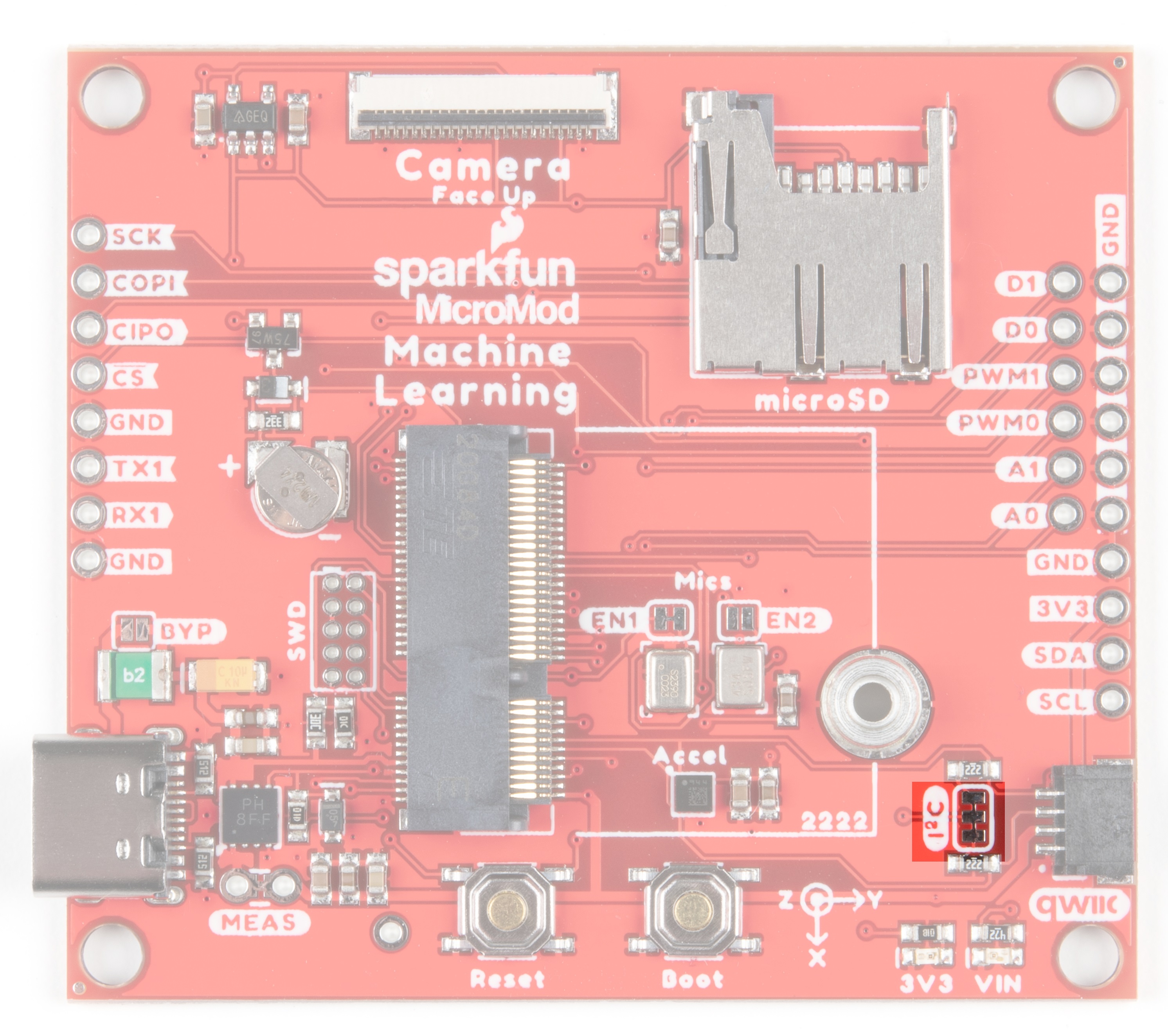
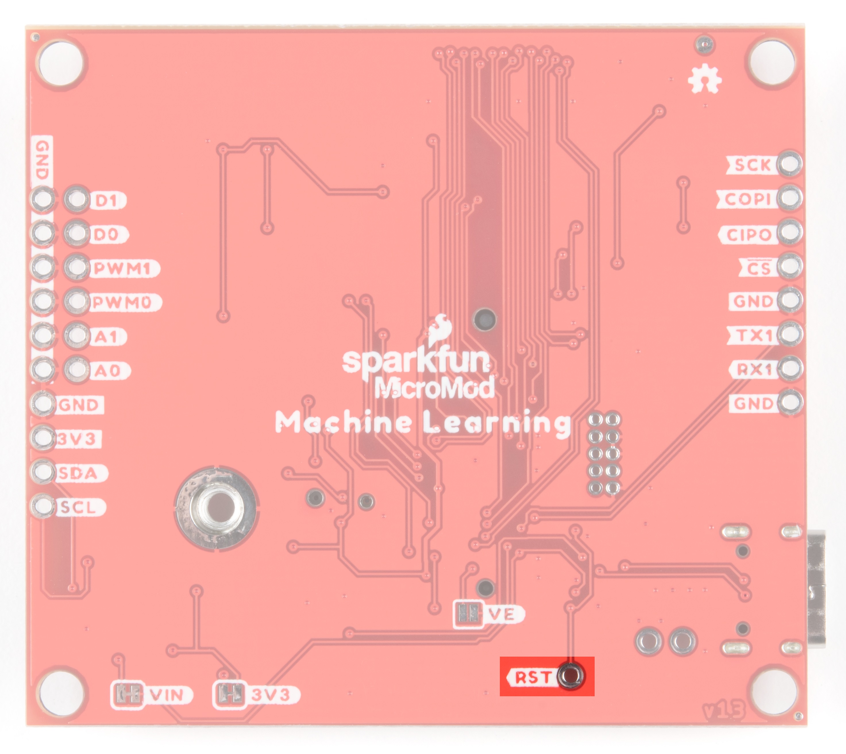
Jumpers
VE Jumper
VIN and 3V3 Jumpers
Cutting these jumpers will disable the VIN and 3V3 LEDs on the front of the board.
I2C Jumper
If you are daisy-chaining multiple Qwiic devices, you will want to cut this jumper; if multiple sensors are connected to the bus with the pull-up resistors enabled, the parallel equivalent resistance could create too strong of a pull-up for the bus to operate correctly. As a general rule of thumb, disable all but one pair of pull-up resistors if multiple devices are connected to the bus. To disable the pull up resistors, use an X-acto knife to cut the joint between the highlighted jumper pads.
RESET PTH
Need an external reset button? These PTH allow you to tie in to the reset functionality.
Machine Learning MicroMod Carrier Pin Functionality
| AUDIO | UART | GPIO/BUS | I2C | SDIO | SPI0 | Dedicated |
| Function | Bottom Pin |
Top Pin |
Function | ||||||
|---|---|---|---|---|---|---|---|---|---|
| (Not Connected) | 75 | GND | |||||||
| 3.3V | 74 | 73 | G5 / BUS5 | ||||||
| RTC_3V_BATT | 72 | 71 | G6 / BUS6 | ||||||
| SPI_CS1# | SDIO_DATA3 (I/O) | 70 | 69 | G7 / BUS7 | |||||
| SDIO_DATA2 (I/O) | 68 | 67 | G8 | ||||||
| SDIO_DATA1 (I/O) | 66 | 65 | G9 | ADC_D- | CAM_HSYNC | ||||
| SPI_CIPO1 | SDIO_DATA0 (I/O) | 64 | 63 | G10 | ADC_D+ | CAM_VSYNC | |||
| SPI COPI1 | SDIO_CMD (I/O) | 62 | 61 | SPI_CIPO (I) | |||||
| SPI SCK1 | SDIO_SCK (O) | 60 | 59 | SPI_COPI (O) | LED_DAT | ||||
| AUD_MCLK (O) | 58 | 57 | SPI_SCK (O) | LED_CLK | |||||
| CAM_MCLK | PCM_OUT | I2S_OUT | AUD_OUT | 56 | 55 | SPI_CS# | |||
| CAM_PCLK | PCM_IN | I2S_IN | AUD_IN | 54 | 53 | I2C_SCL1 (I/O) | |||
| PDM_DATA | PCM_SYNC | I2S_WS | AUD_LRCLK | 52 | 51 | I2C_SDA1 (I/O) | |||
| PDM_CLK | PCM_CLK | I2S_SCK | AUD_BCLK | 50 | 49 | BATT_VIN / 3 (I - ADC) (0 to 3.3V) | |||
| G4 / BUS4 | 48 | 47 | PWM1 | ||||||
| G3 / BUS3 | 46 | 45 | GND | ||||||
| G2 / BUS2 | 44 | 43 | CAN_TX | ||||||
| G1 / BUS1 | 42 | 41 | CAN_RX | ||||||
| G0 / BUS0 | 40 | 39 | GND | ||||||
| A1 | 38 | 37 | USBHOST_D- | ||||||
| GND | 36 | 35 | USBHOST_D+ | ||||||
| A0 | 34 | 33 | GND | ||||||
| PWM0 | 32 | 31 | Module Key | ||||||
| Module Key | 30 | 29 | Module Key | ||||||
| Module Key | 28 | 27 | Module Key | ||||||
| Module Key | 26 | 25 | Module Key | ||||||
| Module Key | 24 | 23 | SWDIO | ||||||
| UART_TX2 (O) | 22 | 21 | SWDCK | ||||||
| UART_RX2 (I) | 20 | 19 | UART_RX1 (I) | ||||||
| CAM_TRIG | D1 | 18 | 17 | UART_TX1 (0) | |||||
| I2C_INT# | 16 | 15 | UART_CTS1 (I) | ||||||
| I2C_SCL (I/0) | 14 | 13 | UART_RTS1 (O) | ||||||
| I2C_SDA (I/0) | 12 | 11 | BOOT (I - Open Drain) | ||||||
| D0 | 10 | 9 | USB_VIN | ||||||
| SWO | G11 | 8 | 7 | GND | |||||
| RESET# (I - Open Drain) | 6 | 5 | USB_D- | ||||||
| 3.3V_EN | 4 | 3 | USB_D+ | ||||||
| 3.3V | 2 | 1 | GND | ||||||
| Function | Bottom Pin |
Top Pin |
Function | ||
|---|---|---|---|---|---|
| (Not Connected) | 75 | GND | |||
| 74 | 73 | CAMERA_D5 | |||
| RTC_3V | 72 | 71 | CAMERA_D6 | ||
| 70 | 69 | CAMERA_D7 | |||
| 66 | 65 | CAMERA_HSYNC | |||
| 64 | 63 | CAMERA_VSYNC | |||
| 62 | 61 | SPI_CIPO | |||
| 60 | 59 | SPI_COPI | |||
| 58 | 57 | SPI_SCK | |||
| CAMERA_MCLK | 56 | 55 | SPI_CS | ||
| CAMERA_PCLK | I2S_SD | 54 | 53 | ||
| PDM_DAT | I2S_WS | 52 | 51 | ||
| PDM_CLK | I2S_SCK | 50 | 49 | BATT_VIN/3 | |
| CAMERA_D4 | 48 | 47 | PWM1 | CAM_VDD | |
| CAMERA_D3 | 46 | 45 | |||
| CAMERA_D2 | 44 | 43 | |||
| CAMERA_D1 | 42 | 41 | |||
| CAMERA_D0 | 40 | 39 | |||
| A1 | 38 | 37 | |||
| A0 | 34 | 33 | |||
| PWM0 | 32 | 31 | |||
| 24 | 23 | SWDIO | |||
| 22 | 21 | SWDCK | |||
| 20 | 19 | RX1 | |||
| CAMERA_TRIG | D1 | 18 | 17 | TX1 | |
| CAMERA_INT | 16 | 15 | |||
| I2C_SCL | 14 | 13 | |||
| I2C_SDA | 12 | 11 | BOOT | ||
| HEADER_CS | D0 | 10 | 9 | VIN | |
| 8 | 7 | GND | |||
| RESET | 6 | 5 | USB_D- | ||
| 3.3V_EN | 4 | 3 | USB_D+ | ||
| 3.3V | 2 | 1 | GND | ||
| Signal Group | Signal | I/O | Description | Voltage | Power | 3.3V | I | 3.3V Source | 3.3V |
|---|---|---|---|---|
| GND | Return current path | 0V | ||
| USB_VIN | I | USB VIN compliant to USB 2.0 specification. Connect to pins on processor board that require 5V for USB functionality | 4.8-5.2V | |
| RTC_3V_BATT | I | 3V provided by external coin cell or mini battery. Max draw=100μA. Connect to pins maintaining an RTC during power loss. Can be left NC. | 3V | |
| 3.3V_EN | O | Controls the carrier board's main voltage regulator. Voltage above 1V will enable 3.3V power path. | 3.3V | |
| BATT_VIN/3 | I | Carrier board raw voltage over 3. 1/3 resistor divider is implemented on carrier board. Amplify the analog signal as needed for full 0-3.3V range | 3.3V | |
| Reset | Reset | I | Input to processor. Open drain with pullup on processor board. Pulling low resets processor. | 3.3V |
| Boot | I | Input to processor. Open drain with pullup on processor board. Pulling low puts processor into special boot mode. Can be left NC. | 3.3V | |
| USB | USB_D± | I/O | USB Data ±. Differential serial data interface compliant to USB 2.0 specification. If UART is required for programming, USB± must be routed to a USB-to-serial conversion IC on the processor board. | |
| USB Host | USBHOST_D± | I/O | For processors that support USB Host Mode. USB Data±. Differential serial data interface compliant to USB 2.0 specification. Can be left NC. | |
| CAN | CAN_RX | I | CAN Bus receive data. | 3.3V |
| CAN_TX | O | CAN Bus transmit data. | 3.3V | |
| UART | UART_RX1 | I | UART receive data. | 3.3V |
| UART_TX1 | O | UART transmit data. | 3.3V | |
| UART_RTS1 | O | UART ready to send. | 3.3V | |
| UART_CTS1 | I | UART clear to send. | 3.3V | |
| UART_RX2 | I | 2nd UART receive data. | 3.3V | |
| UART_TX2 | O | 2nd UART transmit data. | 3.3V | |
| I2C | I2C_SCL | I/O | I2C clock. Open drain with pullup on carrier board. | 3.3V |
| I2C_SDA | I/O | I2C data. Open drain with pullup on carrier board | 3.3V | |
| I2C_INT# | I | Interrupt notification from carrier board to processor. Open drain with pullup on carrier board. Active LOW | 3.3V | |
| I2C_SCL1 | I/O | 2nd I2C clock. Open drain with pullup on carrier board. | 3.3V | |
| I2C_SDA1 | I/O | 2nd I2C data. Open drain with pullup on carrier board. | 3.3V | |
| SPI | SPI_COPI | O | SPI Controller Output/Peripheral Input. | 3.3V |
| SPI_CIPO | I | SPI Controller Input/Peripheral Output. | 3.3V | |
| SPI_SCK | O | SPI Clock. | 3.3V | |
| SPI_CS# | O | SPI Chip Select. Active LOW. Can be routed to GPIO if hardware CS is unused. | 3.3V | |
| SPI/SDIO | SPI_SCK1/SDIO_CLK | O | 2nd SPI Clock. Secondary use is SDIO Clock. | 3.3V |
| SPI_COPI1/SDIO_CMD | I/O | 2nd SPI Controller Output/Peripheral Input. Secondary use is SDIO command interface. | 3.3V | |
| SPI_CIPO1/SDIO_DATA0 | I/O | 2nd SPI Peripheral Input/Controller Output. Secondary use is SDIO data exchange bit 0. | 3.3V | |
| SDIO_DATA1 | I/O | SDIO data exchange bit 1. | 3.3V | |
| SDIO_DATA2 | I/O | SDIO data exchange bit 2. | 3.3V | |
| SPI_CS1/SDIO_DATA3 | I/O | 2nd SPI Chip Select. Secondary use is SDIO data exchange bit 3. | 3.3V | |
| Audio | AUD_MCLK | O | Audio master clock. | 3.3V |
| AUD_OUT/PCM_OUT/I2S_OUT/CAM_MCLK | O | Audio data output. PCM synchronous data output. I2S serial data out. Camera master clock. | 3.3V | |
| AUD_IN/PCM_IN/I2S_IN/CAM_PCLK | I | Audio data input. PCM syncrhonous data input. I2S serial data in. Camera periphperal clock. | 3.3V | |
| AUD_LRCLK/PCM_SYNC/I2S_WS/PDM_DATA | I/O | Audio left/right clock. PCM syncrhonous data SYNC. I2S word select. PDM data. | 3.3V | |
| AUD_BCLK/PCM_CLK/I2S_CLK/PDM_CLK | O | Audio bit clock. PCM clock. I2S continuous serial clock. PDM clock. | 3.3V | |
| SWD | SWDIO | I/O | Serial Wire Debug I/O. Connect if processor board supports SWD. Can be left NC. | 3.3V |
| SWDCK | I | Serial Wire Debug clock. Connect if processor board supports SWD. Can be left NC. | 3.3V | |
| ADC | A0 | I | Analog to digital converter 0. Amplify the analog signal as needed to enable full 0-3.3V range. | 3.3V |
| A1 | I | Analog to digital converter 1. Amplify the analog signal as needed to enable full 0-3.3V range. | 3.3V | |
| PWM | PWM0 | O | Pulse width modulated output 0. | 3.3V |
| PWM1 | O | Pulse width modulated output 1. | 3.3V | |
| Digital | D0 | I/O | General digital input/output pin. | 3.3V |
| D1/CAM_TRIG | I/O | General digital input/output pin. Camera trigger. | 3.3V | |
| General/Bus | G0/BUS0 | I/O | General purpose pins. Any unused processor pins should be assigned to Gx with ADC + PWM capable pins given priority (0, 1, 2, etc.) positions. The intent is to guarantee PWM, ADC and Digital Pin functionality on respective ADC/PWM/Digital pins. Gx pins do not guarantee ADC/PWM function. Alternative use is pins can support a fast read/write 8-bit or 4-bit wide bus. | 3.3V |
| G1/BUS1 | I/O | 3.3V | ||
| G2/BUS2 | I/O | 3.3V | ||
| G3/BUS3 | I/O | 3.3V | ||
| G4/BUS4 | I/O | 3.3V | ||
| G5/BUS5 | I/O | 3.3V | ||
| G6/BUS6 | I/O | 3.3V | ||
| G7/BUS7 | I/O | 3.3V | ||
| G8 | I/O | General purpose pin | 3.3V | |
| G9/ADC_D-/CAM_HSYNC | I/O | Differential ADC input if available. Camera horizontal sync. | 3.3V | |
| G10/ADC_D+/CAM_VSYNC | I/O | Differential ADC input if available. Camera vertical sync. | 3.3V | |
| G11/SWO | I/O | General purpose pin. Serial Wire Output | 3.3V |
Board Dimensions
The Machine learning Carrier Board measures 2.3 inches by 2.05 inches.
