How to Run a 5V Device On a 3.3V System With Qwiic
 Christo-boots with the-pher, santaimpersonator
Hardware Assembly
Breakout Pins
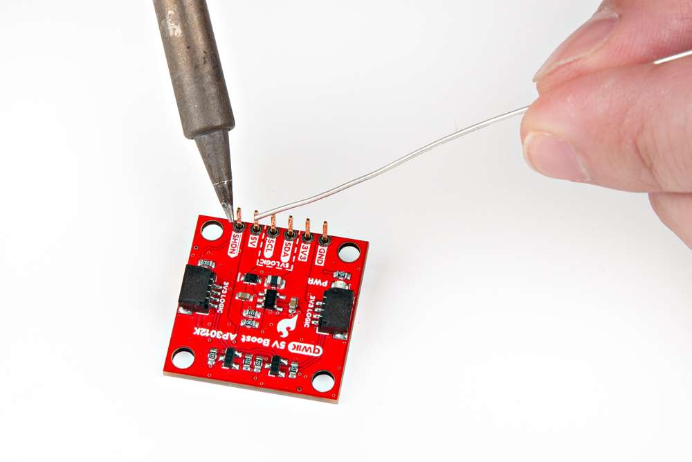
The PTH pins on the Qwiic 5V Boost are broken out into six 0.1"-pitched pins on the edge of the board. These pins are used to connect a 5V I2C device to the Qwiic connect system.
| Headers are versatile option testing and development. | Users can also connect a device directly to the board. |
 |
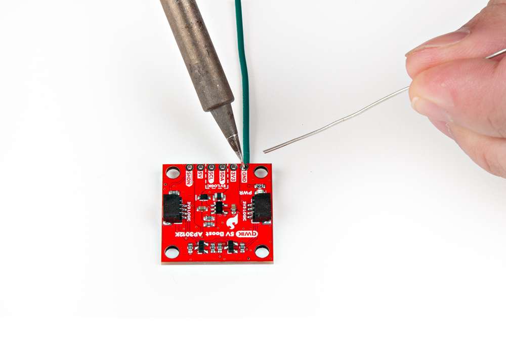 |
| Soldering headers to the Qwiic 5V Boost. | Soldering wires to the Qwiic 5V Boost. |
Tip: If you have never soldered before or need a quick refresher, check out our How to Solder: Through-Hole Soldering guide.
How to Solder: Through-Hole Soldering
Configuration Options: With the 3V3/5V jumpers to configure the logic-levels of the I2C PTH pins, users can convert the power and logic-levels of the Qwiic connector to any combination of 3.3V and/or 5V on the PTH pins. Users will have the following options for connecting a device to the Qwiic 5V Boost:
| Output Power | 5V | 5V | 3.3V |
| I2C Logic-Level | 3.3V | 5V | 5V |
| Power Supply | Logic-Level |
| Use either the 5V or the 3V3 PTH pins to supply 5V or 3.3V power to the device. | Users can modify the 3V3/5V jumpers to configure the logic-level for the SDA and SCL PTH pins.
|
By default, the pins are configured to a 5V logic-level.
Qwiic Connector
The simplest method to connect the Qwiic 5V Boost board to a microcontroller and/or other Qwiic devices, is through the Qwiic connector.
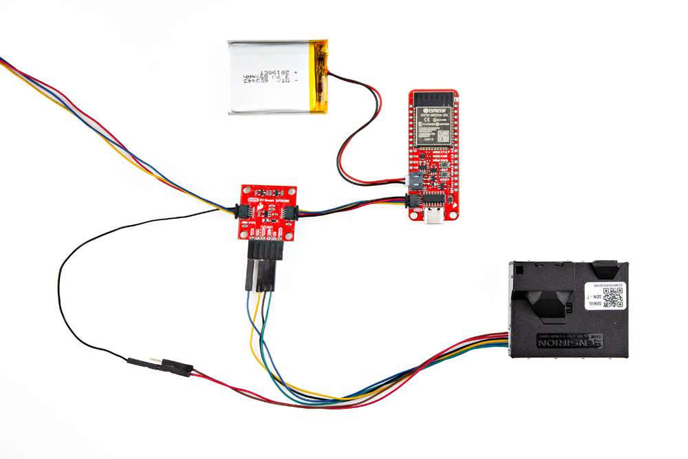
Tip: The intended design of the Qwiic 5V Boost board was to be utilized with the Qwiic connector system. However, the Qwiic 5V Boost can also be utilized with other interfaces, similar to how the SparkFun Logic Level Converter - Single Supply operates. The only difference is its TTL conversion, which is push-pull and not open-drain.