How Does an FPGA Work?
Introduction
Let’s start at the beginning. What is an FPGA? Well, FPGA stands for Field Programmable Gate Array, which isn’t helpful in understanding what they are or do but we had to get that out of the way.
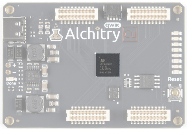
FPGAs belong to a class of devices known as programmable logic, or sometimes referred to as programmable hardware. Essentially, an FPGA doesn’t do anything itself but it can be configured to be just about any digital circuit you want. The magic here is that nothing physically changes. You simply load a configuration into the FPGA and it starts behaving like the circuit you wanted. No soldering, no jumper wires, no fuss. An FPGA can then be reconfigured to behave like another circuit, and another, and another. The configuration is RAM based which means it can essentially be reconfigured an unlimited number of times.
 |
 |
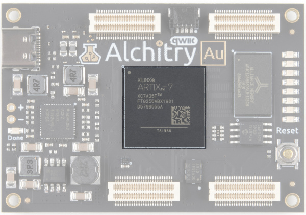
| Lattice iCE40 HX FPGA highlighted on the Alchitry Cu Board | Xilinx Artix 7 FPGA highlighted on the Alchitry Au Board |
Even though we talk about using FPGAs to create digital circuits, you don’t typically draw schematics to create designs for them. The size and complexity of the circuits FPGAs can contain would become very cumbersome should you actually draw out a schematic. Instead, you can describe the behavior of the circuit you want and the tools will use this to create a circuit that matches that behavior.
In this regard it can feel like programming since you are just typing text. However, the fundamental implementation is drastically different as you are creating hardware.
If creating hardware with text seems like magic, don’t worry. The way they work is actually quite simple in concept and in this tutorial we are going to really break it down.
Suggested Reading
In this tutorial we are going to explore what an FPGA is and how they work. I’m going to assume you have a decent understanding of electricity (voltage, current, etc) and binary values. Everything else will be quickly built upon the basics. This is intended as an overview of what an FPGA is and its fundamental design, not a guide to designing your own.
If you aren’t familiar with the following concepts, we recommend checking out these tutorials before continuing.
Voltage, Current, Resistance, and Ohm's Law
What is Electricity?
Analog vs. Digital
Transistors
Digital Circuits and Logic Gates
Digital Circuits
One caveat of FPGAs is that they can only create digital circuits. Some of the newer FPGAs include on-board analog to digital converters, but even these convert the analog input into a digital signal as soon as possible. But what is a digital circuit?
In electronics, digital is used to describe circuits that abstract away continuous voltage values in favor of discrete 1s and 0s. The actual voltages used and the thresholds don’t actually matter for the higher level design but you will often see something like 0V being a 0 and 1.2V being a 1 inside the FPGA. If the actual voltage is, say, 0.8V that is close enough to 1.2V to be considered a 1 and everything works the same.
A digital circuit is designed to push the voltages to the extremes which makes them incredibly resilient to noise and other real-world interference. The concept of digital also gives us a way to design complicated behavior into the circuit without having to worry about the lower level design. We get to work in an ideal world. The nitty gritty is taken care of in the design of the simple building blocks that we will be using.
These building blocks are logic gates.
Logic Gates
There are a handful of different logic gates but the most common ones are AND, OR, XOR, and NOT. Each of these takes digital inputs, performs its logical function, and outputs a digital value.
An AND gate takes two inputs and outputs a 1 only when the first input and the second input are 1. If either input is 0, the output is 0. The symbol of an AND gate looks like this:
An OR gate takes two inputs and outputs a 1 when either the first input or the second input is 1. Only when both are 0 is the output 0. Here’s the OR gate symbol:
An XOR gate is similar to an OR gate but only outputs a 1 when either the first input or the second input are 1, but not when both are 1. It can also be thought of as outputting a 1 when the inputs are different. The X in XOR stands for exclusive. Here is its symbol:
A NOT gate is the simplest gate. It has one input and simply outputs the opposite of whatever it is. So a 1 becomes a 0 and a 0 becomes a 1.
There are variations of the basic gates known as NAND, NOR, and XNOR. These are simply the standard versions with their outputs inverted.
Just for some extra context, an AND gate, like all logic gates, can be built using transistors. The image below shows an example of how an AND gate could be implemented. The schematic uses NMOS and PMOS MOSFET transistors. This type of design is known as CMOS (complementary metal-oxide semiconductor) and is what is used in most modern circuits.
Note that the above schematic is actually a NAND gate followed by a NOT gate. This is because CMOS circuits invert the output.
Multiplexers
Now that we have the basic building blocks from transistors to logic gates, we can make something more useful with them. With just logic gates, you can describe any digital circuit. However, there are many reoccurring higher level functions that get their own symbols such as those used for binary math (adders, multipliers, etc).
We are going to look at one of the fundamental building blocks of FPGAs, the multiplexer.
A multiplexer selects a single input out of set based on the value of its select input. Here is its symbol:
The / on the sel line is used to show it is 6 bits wide.
The number of inputs will vary but the multiplexer always just has one output.
The way the select input is encoded will also vary. Usually, you will see it as a binary number, but the simpler circuit uses a one-hot encoding. A one-hot encoding is simply a binary value where there is always exactly one 1. The position of the 1 is the important thing.
A decoder takes a binary value and turns it into a one-hot signal. An encoder turns a one-hot value into a binary number. These can be used to make a one-hot multiplexer accept binary values.
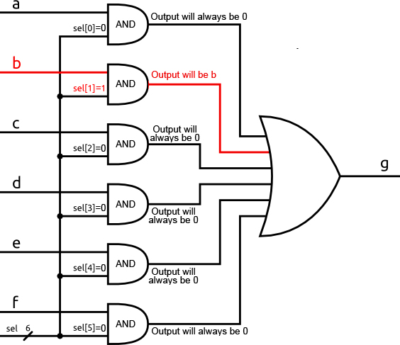
Take a look at how we could implement a one-hot encoded multiplexer using just some AND and OR gates.
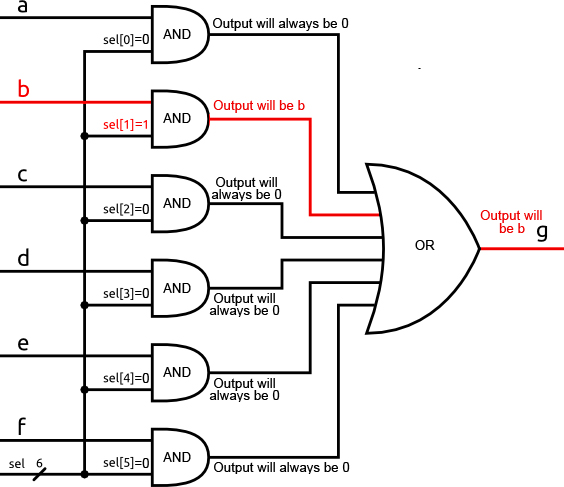
If we set the sel value to be 000010, meaning only sel[1] is 1, then we can see that for every AND gate, except for the one with the b input, one of the inputs will be 0. That means that each of those will always output 0 regardless of what the inputs a, c, d, e, and f are. The only input that matters is b. When b is 1, it is AND’d with a 1 and the output of the AND gate is 1. When b is 0, it is AND’d with 1 and the output of the AND gate is 0.
In other words, the output of the AND gate is simply b.
The OR gate in this schematic is shown with more than two inputs. This can be created by creating a tree of two input OR gates where two inputs are OR’d together and the outputs are then OR’d together over and over until you have one output. A multi-input OR gate behaves just as you would expect with the output being 1 if any of the inputs are 1.
However, in this circuit every input to the OR gate is guaranteed to be 0 except the input from the AND gate whose output is b. This means that the OR gate will simply output a 1 when b is 1 and a 0 when b is 0.
In other words, the output of the OR gate is simply b.
You could repeat this logic for any input and, as long as the input is one-hot, the input that corresponds to the given 1 will be passed through to the output.
You can imagine having a large matrix of multiplexers with a programmable sel input. This would allow you to route signals wherever you needed in your design. This is how FPGAs get their signals where they need to be and it is called the general routing matrix.
Obviously the details for routing thousands and thousands of signals gets messy, but fundamentally it is just using a bunch of multiplexers with select inputs connected to programmable memory.
Look-Up Tables
So now that we have a way to dynamically route signals wherever they need to be, we need a way to perform arbitrary logic. We will again be using multiplexers, or rather a descendant of them known as LUTs or look-up tables.
Imagine we have a multiplexer with four inputs and a 2 bit binary select (instead of one-hot). Now, instead of exposing the main inputs to the world, let’s hook them up to some programmable memory. This means we can program each input to some constant value. Wrap this all up into a block and we have a two input LUT.
The two inputs to the LUT are the select inputs of the multiplexer. By programming the multiplexer inputs to be whatever we want, we can use this LUT to implement ANY two-to-one binary function.
For example, we could make it act like a simple AND gate by setting the contents of the memory to be as follows.
| Address (In[1:0]) | Value (Out) |
|---|---|
| 00 | 0 |
| 01 | 0 |
| 10 | 0 |
| 11 | 1 |
This is a simple example - normally LUTs are bigger than just two inputs and the FPGA on the Alchitry Au is based around five input LUTs.
Xilinx actually puts two five input LUTs together with another multiplexer to create either a six input LUT or a five input LUT with two independent outputs.
If you want to really dive into what the LUTs and resources in the FPGA look like, check out this document from Xilinx on the Artix 7. This document is very dense. You’ve been warned. Page 20 is worth a glance though. It shows a simplified schematic of a SLICEL. Slices are one building-block above LUTs. The four boxes on the left are the LUTs like shown above.
For some context, the FPGA on the Alchitry Au has 20,800 dual LUTs. That’s a lot of LUTs but not even close to the largest FPGAs available which have about 260x that amount at the time of writing. As you can imagine, the routing of all those signals alone is insanely complex. Luckily for us, to use FPGAs you don’t need to do any of that. The tools take care of all the low level routing and LUT programming. We just get to describe the circuits we want.
Why Use an FPGA?
Hopefully this tutorial has given you a warm fuzzy feeling for how FPGAs actually work, but why would you use one?
Usually when this question comes up it's in the context of choosing between using a processor or creating a custom design with an FPGA. Lots of people know how to code, far fewer understand how to create designs for FPGAs. Writing code is often easier to create complex behavior and to drastically change how something is implemented.
However, FPGAs can be far more efficient in terms of processing time as well as offering very tight timing. To illustrate this, let’s look at a trivial example of turning an LED on when you press a button. If you wrote code to do this with something like an Arduino, the processor would run a small loop of code that would read the state of a pin then update the state of another pin based on that value.
If you optimized the code you could probably get this to update in the millions of times per second. That may sound great but let’s look at what it would look like with an FPGA. In the case of simply connecting a button to an LED with an FPGA, you simply connect the button and the LED. The value from the button passes through some input buffer, is fed through the routing matrix, then output through an output buffer. This process happens continuously all the time. The only delay comes from the switching delays of the transistors in the chip, which are incredibly small.
To expand on this, let’s now add a microphone to our design. We could take samples from the microphone and do some processing on it to figure out the frequencies in the captured audio. From some first hand experience, I know this is pretty hard to do on a small microcontroller in real time with any decent sampling rate. The processor needs to juggle reading in samples from the microphone, storing them in some buffer, performing a bunch of math, then output the values to maybe a display of LEDs. Each of these steps takes time and the processor can only really do one at a time.
With an FPGA, you could dedicate a small piece of your design to reading in samples from the microphone. This could then hand off the samples to a buffer, which, when full, would hand them off to a circuit that would do the calculations. That circuit could then hand off the results to another circuit that would display them on some LEDs.
Each of these stages would operate entirely independently from one another since they simply exist in hardware. They aren’t lines of code competing for processor time.
Now imagine we still want the button hooked up to the LED. Our previous spectacular response time of a millionth of a second is now an abysmal fifth of a second because we can’t spare the processor time to read the button that often. However, in the FPGA the button and LED are still just connected together and responding at the near instantaneous speed as before.
This independence makes FPGAs a fantastic candidate for controlling anything that requires tight timing. For example, the WS2812B LED (aka NeoPixel) requires a tightly timed stream of pulses to write data to them. When you use a microcontroller, you usually need to write some inline-assembly just to get the timing of the pulses to be accurate enough. You also need to disable interrupts as any stalls would be detrimental to the signal.
With an FPGA, it is simple to create a series of tightly controlled pulses to drive these LEDs and you don’t need to worry about anything else in your design conflicting with the timing.
When to Use an FPGA
Given all the pros of using FPGAs, you may be asking yourself “Why wouldn’t I use one for everything!” Great question!
In the description of how FPGAs work, you may have noticed that there's a lot of extra "stuff" that has to go on to implement even the simplest circuit dynamically. This isn’t without its cost, and I mean that both in $$$ and in design resources.
FPGAs tend to be expensive. The larger ones easily go for tens of thousands of dollars PER CHIP. This is due to the amount of silicon required to make them, the huge amount of RnD to design the chips and the tools, and the relatively low volume compared to things like tiny processors used in phones.
Another cost is power. There are a lot of transistors used in the LUTs compared to the number needed to implement the circuit directly. All these transistors require power to operate. Because of this, FPGAs tend to be poor candidates for battery operated devices. You can of course design your circuits to be power efficient but even doing absolutely nothing, the FPGA on the Alchitry Au consumes a little over 100mA. You can easily get over 1000mA if you start pushing the chip. As a comparison the ATmega32U4, the chip used on the Arduino Leonardo, uses 27mA when running with 5V at full speed. Granted the Alchitry Au is substantially more capable.
So why use FPGAs at all? Well, you have two major alternatives to creating a custom digital circuit. First, you could build it yourself out of discrete logic. This would take a significant amount of time, likely cost significantly more, and have little flexibility if you needed to change something.
The second, and more realistic, alternative is to create the circuit directly in silicon. This creates a very fast, very efficient circuit, but at the cost of zero flexibility and truck loads of $$$. Custom silicon has huge upfront costs associated with the tooling and setup. The incremental cost per chip would be lower than individual FPGAs though. However, unless you’re making tens of thousands of chips, this will be more expensive overall. Even then, it sometimes doesn’t make sense to lock your design into silicon. With an FPGA you can change it whenever you need to without penalty.
Because of their flexibility and low-cost compared to the alternatives, FPGAs open the doors to adding custom digital circuits to just about any design. But, do you really need a custom circuit?
It is important to keep in mind that FPGAs are just like any other tool. A hammer is great for nailing in nails, but it is terrible for screwing in screws. Just as trying to nail a nail with a screwdriver would be quite futile.
Creating custom circuits can be difficult and you often need to ask yourself if there is a better solution. There are many very capable processors with tons of peripherals that can handle most of the problems you need to solve. Trying to do something like sending and receiving data over WiFi would be a daunting task with an FPGA but is easily accomplished with a few dollar microcontroller like the ESP8266.
I often describe FPGAs as an assembly line. Each station on an assembly line works independent from each other and they are incredibly efficient at what they are designed for. However, it can be difficult to initially set up the line and if you want to make major changes it is often easier to start from scratch.
On the other hand, processors are like people. A single person could do just about any task given enough time and the training. Complex sequential tasks are easy for a person to accomplish.
Do you really want to set up an entire sandwich manufacturing plant just to make you a sandwich for lunch?
FPGAs are amazing and often indispensable for the tasks they excel at but they are just another tool to add to your toolbox. A very powerful and worthwhile tool to invest in, but still just another tool.
Troubleshooting
If your product is not working as you expected or you need technical assistance or information, head on over to the Alchitry Forums. This is a great place to do some initial troubleshooting as well as to find and ask for help.

Resources and Going Further
These are the basics of how FPGAs work and what they are made of. Alchitry's website has more great resources, including tutorials, projects, and the Alchitry Forum.
- Alchitry
- Alchitry Au+ Schematic (PDF)
- Alchitry Au Schematic (PDF)
- Alchitry Cu Schematic (PDF)
- Xilinx Artix 7 User Guide
If you'd like to delve deeper into the world of FPGAs and Lucid, check out "Learning FPGAs: Digital Design for Beginners with Mojo and Lucid HDL" by Justin Rajewski. It's available on Amazon and is a great resource for understanding and ultimately designing your own FPGAs.
We are continually expanding our offering of tutorials and products related to FPGAs. Check out some of the following tutorials!
Programming an FPGA
First FPGA Project - Getting Fancy with PWM
External IO and Metastability


