External IO and Metastability
Introduction
If you’ve gone through the first couple of Alchitry tutorials, you may have been wondering how the inputs and outputs of the top-level module know where to connect on the board. What about the LED name tells the tools what pin on the FPGA to use? Well wonder no more! In this tutorial I’m going to explain the basics of constraint files and dive into some of the dangers of using external signals in your designs.
Required Materials
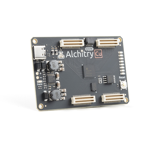
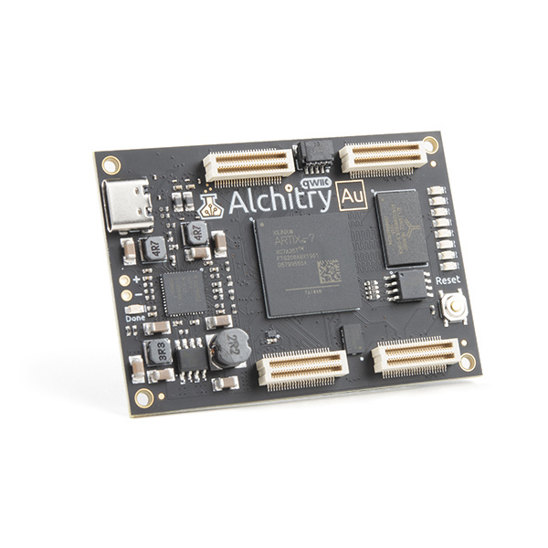
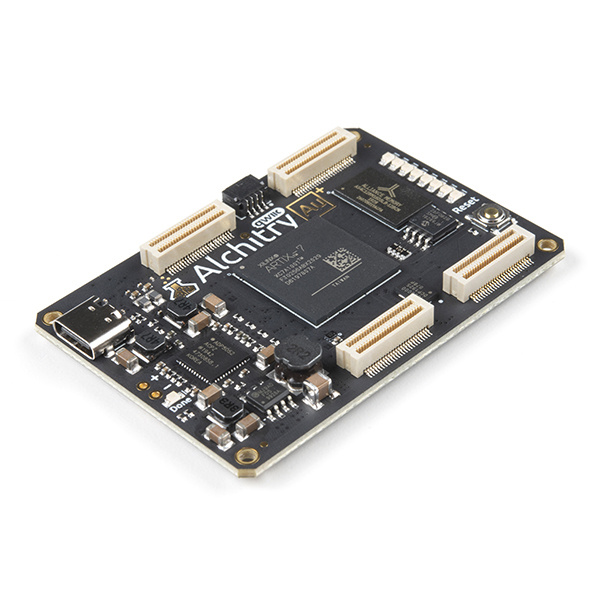
This tutorial is primarily conceptual, but if you'd like to follow along, you'll need the following materials.
Suggested Reading
If you aren’t familiar with the following concepts, we recommend checking out these tutorials before continuing.
Programming an FPGA
How Does an FPGA Work?
First FPGA Project - Getting Fancy with PWM

Constraint Files
Constraint files are used to specify specific design constraints that are FPGA specific. There isn’t a current standard for the use of these as each FPGA manufacturer wants to allow different features.
Pin Locations
The most common use for these files is constraining a top-level input or output to a physical pin and to make this easy, Alchitry Labs supports Alchitry Constraint Files or ACFs. These have a very simple syntax and will work for either the Au or Cu.
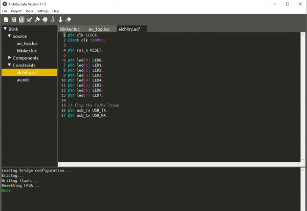
If you create a new project for either board, under the Constraints header in the project navigator you’ll find a file called alchitry.acf. This file contains the basic pinout definitions for the board. This is the Alchitry Constraint File for the project we created in the Alchitry PWM tutorial.
Looking closer at this file, you'll see the following (or something very similar):
pin clk CLOCK;
clock clk 100MHz;

pin rst_n RESET;

pin led[0] LED0;
pin led[1] LED1;
pin led[2] LED2;
pin led[3] LED3;
pin led[4] LED4;
pin led[5] LED5;
pin led[6] LED6;
pin led[7] LED7;

// flip the Tx/Rx lines
pin usb_rx USB_TX;
pin usb_tx USB_RX;
The syntax for a pin location definition is pin signal PIN; where signal is the name of the input or output in your top-level module and PIN is the physical pin to connect it to. You can also put the optional pullup or pulldown keyword after the pin name but before the semicolon to specify if the on-chip pullup or pulldown resistor should be enabled. These are only for inputs. Also note that the Cu doesn’t support pulldowns and the keyword will be ignored.
Alchitry Labs defines some special pin names for the signals on the board such as RESET and LED0. These are useful since they map to different physical pins on the Au and Cu but the tools know which pin to use.
All the broken out IO pins also have convenient names using the format of the bank letter followed by the pin number.
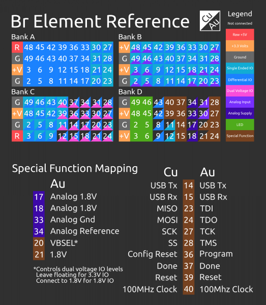
The pinout of the Br Element looks like this.
Bank A is the top left connector when looking at the board with the USB port on the left. Bank D is the bottom right. Basically, the same layout as the reference sheet.
If you want to use, say, pin 2 of bank A, you would use the pin name A2. This name is the same regardless if you are using the Au or Cu. These names then get mapped to the physical pin of the FPGA chip by the tools.
The top left corner of each square corresponds to the Cu’s pin’s capabilities and the bottom right half is the Au’s. These halves are sometimes split again if there are multiple uses for a pin.
For example, pin A20 can be used as a differential signal with the Au but only as a single ended signal on the Cu. Pin B2 can be an analog input or a differential signal on the Au but only a single ended signal on the Cu.
Also note that all differential IO can be used as single ended IO as well.
Banks A and B are fully loaded on the Au and Cu while bank C is only partially loaded on the Cu and bank D is mostly special signals.
The second half of the reference sheet is the signal mapping for bank D. For example, D14 is the USB Tx signal on both the Au and Cu.
All the analog signals and dual-voltage select signals are only on the Au and aren’t connected to anything on the Cu (noted by the black top left of the square).
Clock Definitions
When you have a clock input in your design, you need to tell the tools how fast the clock runs. This can be done in the Alchitry Constraint File as well using the clock signal frequency; syntax.
For the clock built onto the board, clock clk 100MHz; is used to specify that it is 100MHz.
This is important so that the tools know how fast your design needs to run. Without this, they don’t know what timing requirements to meet when laying out your design.
Other Constraint Formats
If you want to specify more advanced constraints, you can add Xilinx or Lattice specific constraint files to your projects for the Au or Cu respectively.
If you make an Au project, you’ll actually already have a Xilinx Design Constraint file called au.xdc in your project. This file has information telling the tools what voltages are used, and some info about the flash holding the FPGA’s configuration.
If you want to really dive into it, you can read Xilinx’s documentation here or click on the button below.
Typically, you will never have to mess with these unless you start doing some really advanced stuff.
Lattice’s constraints are split into PCF and SDC files. PCF stands for physical constraint file and is used to define the pinout and SDC stands for clock design constraint is used to define the clock frequencies.
Refer to the iCEcube2UserGuide - specifically chapters 5 and 6 - for more details.
Again, you shouldn’t need to write these yourself if you are using Alchitry constraints.
Metastability
Now that you know how to define the pinout for your design, we should get into the dangers of using external signals.
For most of your design, a signal starts and ends inside the FPGA. When this happens the tools can accurately manage the timing of this to make sure everything works as expected. However, external signals aren’t controllable and without special care can cause your entire design to behave unexpectedly.
This happens due to a phenomenon called metastability.
Metastability is when your nice digital system stops working in 0s and 1s and gets stuck somewhere in between or even oscillating between values.
This can happen when you violate specific assumptions made by the DFFs (we covered these back in the Programming an FPGA tutorial).
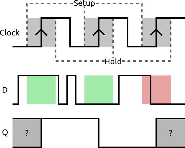
The main assumption is that the D input of any DFF will be stable for a certain amount of time before and after the rising edge of a clock. The time requirement before is called the setup time and the time after is called the hold time.
If the D input changes in this window, the DFF can fail to capture the value and may become unstable.
Here is a diagram illustrating this:
The first two edges of the clock have no D transitions around them so the value of D is correctly saved and output on Q. However, the last one has a transition near the rising edge so the output becomes unpredictable.
The easiest solution to this problem is to simply respect the setup and hold windows. This can be done when you use a clocked bus like SPI. However, for anything that isn’t clocked, you can’t predict or control when the signal will change.
Imagine trying to get a user to avoid 100,000,000 tiny windows per second when pushing a button. It’s impossible.
The workaround for this is chaining two or more DFFs together:
This significantly reduces the likelihood of the output of the second DFF being unstable. It does introduce a small amount of latency into the input though. It’s important to know this doesn’t solve the problem of metastability. It merely drastically reduces the chance of it being an issue. Adding more DFFs to the chain further reduces the probability of it becoming an issue but the amount quickly diminishes and two is usually plenty.
There is a component in the Component Library called pipeline that can be used to synchronize inputs. It is under the Miscellaneous category. It simply pipes an input through a parameterized number of DFFs before outputting it.
module pipeline #(
    DEPTH = 1 : DEPTH > 0 // number of stages
  )(
    input clk,  // clock
    input in,   // input
    output out  // output
  ) {

  dff pipe[DEPTH] (.clk(clk));
  var i;

  always {
    // in goes into the start of the pipe
    pipe.d[0] = in;

    // out is the end of the pipe
    out = pipe.q[pipe.WIDTH-1];

    // for each intermediate state
    for (i = 1; i < DEPTH; i++)
      pipe.d[i] = pipe.q[i-1]; // copy from previous
  }
}
You may have noticed in the previous tutorials that a component called the reset_conditioner is used to condition the reset signal (who would’ve guessed?!).
This component takes care of two things. First, it synchronizes the reset button to the clock. Second, it ensures the reset signal stays high for a minimum amount of time. These two requirements are important for ensuring that the signal is clean and the entire FPGA comes out of reset at the same time.
module reset_conditioner #(
    STAGES = 4 : STAGES > 1 // number of stages
  )(
    input clk,  // clock
    input in,   // async reset
    output out  // snyc reset
  ) {

  dff stage[STAGES] (.clk(clk), .rst(in), #INIT(STAGESx{1}));

  always {
    stage.d = c{stage.q[STAGES-2:0],0};
    out = stage.q[STAGES-1];
  }
}
The way this works is clever. It uses four DFFs in a chain with the first one getting a constant 0 input on D. The raw reset signal is used to reset these four DFFs to 1. When they aren’t being forced to 1 by the reset, they will output 1 for the first four clock cycles then drop the output low to allow normal operation of the reset of the design. This means that the reset signal will be at least four clock cycles long and will end synchronized to the clock.
This design is from Xilinx’s whitepaper entitled Get Smart About Reset: Think Local, Not Global. This is a great read - in addition to discussing the design of the reset, it also talks about the cost of using a reset. Basically, if you don’t need a DFF to be reset, don’t connect the reset signal to it. It just requires extra routing resources and complicates your design. Many DFF values don’t matter when a design is reset as they will get assigned a known value almost immediately.
Multiple Clocks
Another area you can run into metastability issues is crossing clock domains. This is when your design has multiple clocks of different frequencies. You can’t simply connect the output of a DFF being clocked at 33MHz to one being clocked at 100MHz. There will be times when timing is violated and bad things happen.
To cross clock domains you have a few options. The first is to use a chain like before. This is the easiest way but isn’t suitable for multi-bit or rapidly changing signals. It is best used for single bit flags.
The more robust and complicated solution is to use an asynchronous FIFO. These are FIFOs that have read and write ports with independent clocks. You can write values to the FIFO from one clock domain and read them out from the other.
This is in the component library under Memory/Asynchronous FIFO.
These work great for getting data across clock domains but you need to ensure that you are reading data from them as fast as you are writing it so they don’t overflow.
The best way, if possible, is to just avoid multiple clocks. You can often create slower parts of your design by simply using a counter to tick when you should do something. This allows the tools to still manage all the timing requirements for you.
This isn’t always possible and when you need to cross clock domains you simply need to take a bit of extra care.
Troubleshooting
If your product is not working as you expected or you need technical assistance or information, head on over to the Alchitry Forums. This is a great place to do some initial troubleshooting as well as to find and ask for help.

Resources and Going Further
Alchitry's website has more great resources, including tutorials, projects, and the Alchitry Forum.
- Alchitry
- Alchitry Au+ Schematic (PDF)
- Alchitry Au Schematic (PDF)
- Alchitry Cu Schematic (PDF)
- Xilinx Artix 7 User Guide
User Guides and Whitepapers:
- Vivado Design Suite User Guide - Using Constraints
- iCEcube2UserGuide
- Get Smart About Reset: Think Local, Not Global
If you'd like to delve deeper into the world of FPGAs and Lucid, check out "Learning FPGAs: Digital Design for Beginners with Mojo and Lucid HDL" by Justin Rajewski. It's available on Amazon and is a great resource for understanding and ultimately designing your own FPGAs.
We are continually expanding our offering of tutorials and products related to FPGAs. Check out some of the following tutorials!
Programming an FPGA
How Does an FPGA Work?
First FPGA Project - Getting Fancy with PWM

