Constant Innovation in Quality Control
Introduction
Here in Quality Control, we are constantly challenged to create fast, thorough, and reliable test procedures. We are never willing to sacrifice any of these three ingredients, and so, the only way to speed up a test is to hire more technicians or... innovate. In our true boot-strapping style, we have always done our best to do the latter.
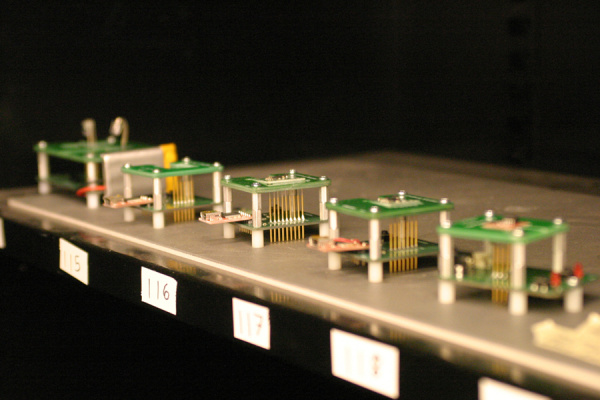
In 2009, we began designing our testing equipment using pogopins.
You can read more about that here: PogoBeds: SparkFun Production and Testing
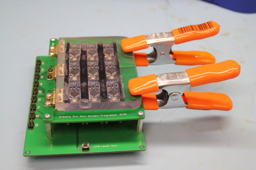
In 2011, we hacked together a multiple board programmer using our first ever waffle press.
You can read more about that here: Ganged Programming with AVR ISP MKIIs
Since then, we have made tons of advancements in our hardware, code, inspection processes, and board layout. In this article, we are going to share some of our best ideas from the past few years. We hope they will help you design better projects and maybe even think about your hardware design in new ways.
Cheers to making great electronics and how to test them!
Multi-Board Programming
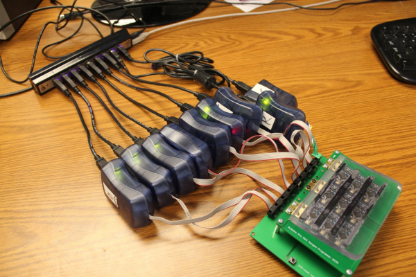
Our first approach to multi-board programming involved multiple programmers, a USB hub, a bunch of cables, and some tricky batch file action.
It sure did speed up our production runs. Nine at a time was a huge improvement from our previous single board programming methods. But, as with most of our testing equipment, it eventually became out-dated, and we wanted to upgrade it.
It became a bit of a hassle to setup -- ensuring that everything was plugged in properly. And over the years, the ribbon cables began to wear out. In November of 2011, we posted a very thorough tutorial on how this ganged-programmer works. Click HERE to check that out. In addition to the hardware design ideas, it actually was a great exercise in using batch files.
About a year after the release of the above programmer, we started having a lot of our technicians computers freeze up mid programming. The famous blue screen of death was happening far too often. We replaced the USB hubs with better quality hubs, and this seemed to help the problem a bit. However, we knew another approach was needed.
We wanted to find a way to program multiple boards simultaneously using one single programmer. Our first thought was to use some sort of amplification or buffer on the programming lines.
To program an AVR using ISP, there are 6 connections that need to be made from the programmer to the target IC:
- VCC
- GND
- RESET
- SCK
- MISO
- MOSI
Experimenting with our logic level converter, we were able to get a few boards to program off one single programmer. Our initial hardware was as follows.
Physically bussing (as in metal connections on the same net) for the GND, VCC and RESET.
SCK and MOSI needed to be buffered, because these signals were being sent to multiple targets. It seemed that the MKII did not have enough output impedance to program multiple targets, so we sent them through the logic level converter. This way, the signal strength was relying on the HIGH logic pin of the converter and not the output of the MKII.
The MISO line was a little trickier. This line carries communication from the target back to the programmer. And if you have a few targets all trying to talk back to the programmer at the same time, the programmer would not understand the returning data. The solution we found was to have only one single target IC talk back to the programmer. This way, the programmer thought it was only talking with one IC and the remaining target ICs on the bus would simply listen along. We figured we could test the solder joint on the remaining ICs MISO lines with some sort of other testcode later.
Above is a picture of the first testing hardware to include a buffered programming circuit. It was used for the Arduino Pro Mini. It could program six boards at a time and lived a decent life on the production floor. If you look closely at the top left you can see the prototyping board and logic level converter used on the programing lines. Unfortunately, this is the best picture I could dig up. It has since been upgraded to a new version (that includes a hex converter buffer circuit). The original hardware pictured above must have been tossed into our electronics recycling.
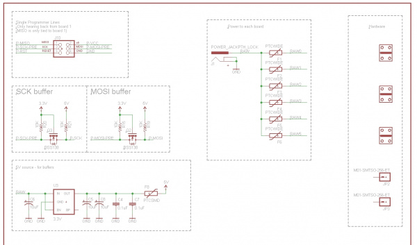
We then incorporated the transistor buffer into the testbed PCB, as show below in the this section of the schematic:
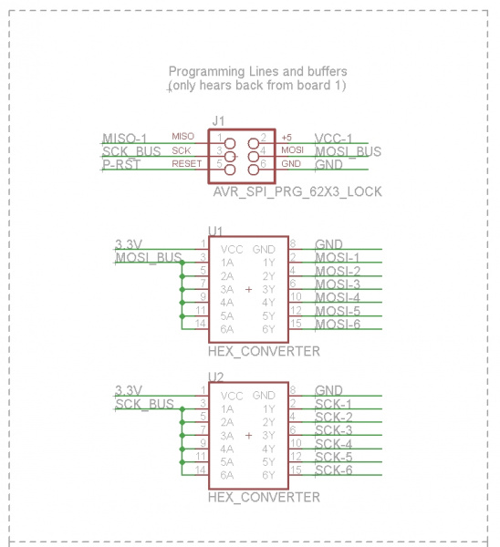
The latest models in production incorporates a hex converter to amplify the SCK and MISO lines like so:
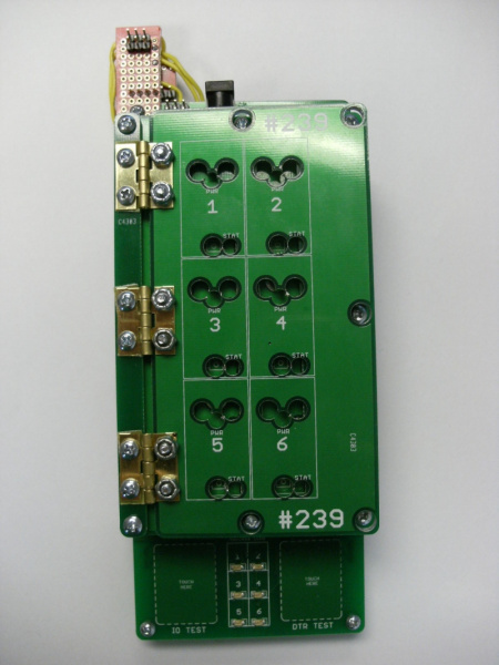
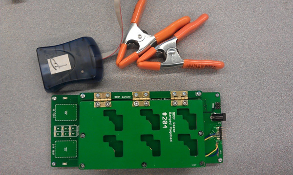
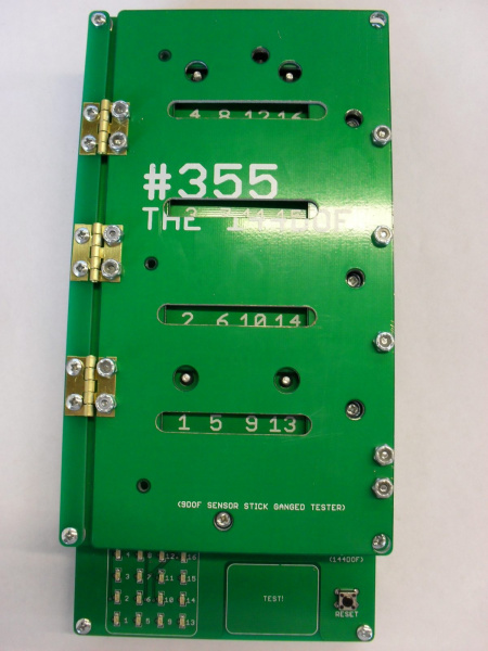
Below is a picture of the latest ganged programmer for the 9 Degrees of Freedom - Razor IMU. It programs six boards at a time and only uses one programmer.
It also has some other advancements including the waffle top, capsense buttons and more. The next few sections of this article are dedicated to some of these other improvements. Read on to learn more.
The Waffle Top
Holding a board in place (on top of pogopins) has always proven to be quite a challenge. We have eventually settled on two approaches: Nubbins and Waffle tops.
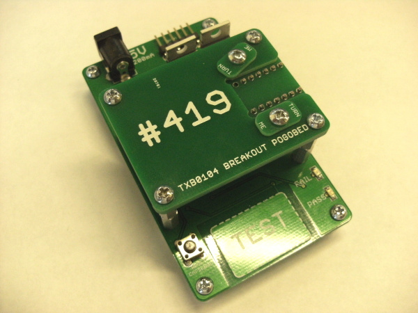
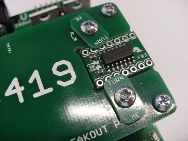
For our testbeds with minimal pogopins (usually a single board tester), we use a little device that we have termed, a "locking nubbin". Basically, it is a small oval shaped piece of PCB with a drill hit in the center. These nubbins sit close the the edge of the frame layer. Below is a picture of a fairly new testbed design that tests our TXB014 Breakout.
This next picture shows the board under test in place. Notice how the nubbins turn and hold the board down on top of the pogopins.
The second approach is what we like to call, "the waffle top". We use this solution for our larger testbeds that require more surface area and pressure to hold the board (or panel) in place.
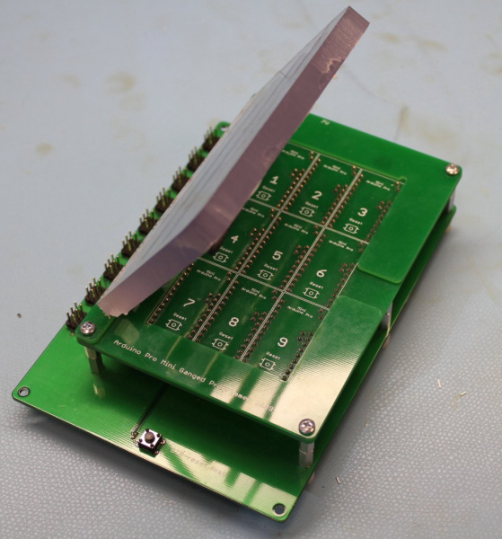
It involves using a flat board of sorts (below shows an example made from acrylic). The waffle top is designed to sit on top of the board (or panel of boards) under test. It is connected to the edge of the testbed with hinges to keep it aligned. This hinged connection also makes it easy to lift away while moving the board-under-test in and out. It's actually quite similar to how a waffle iron works, hence the name.
Below is a picture of the first waffle top. It was made from acrylic and used on the testbed for our Arduino Pro Mini 328 - 5V/16MHz.
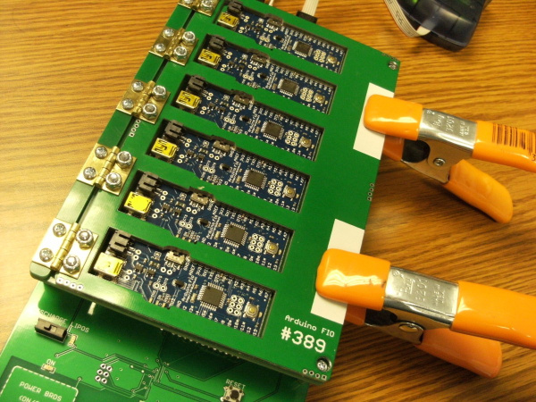
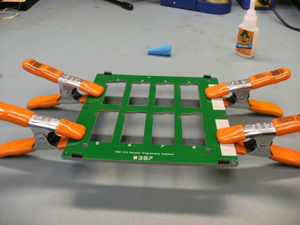
We found that ordering two PCBs and glueing them together has proven to be a much easier method for us these days. Pictured below is our testbed for the Arduino FIOs.
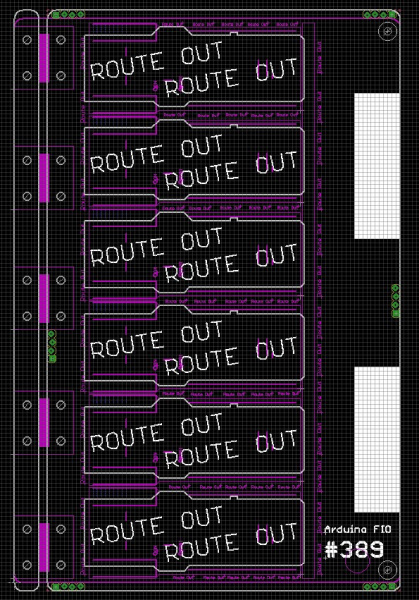
Notice that it also has cut-out areas to allow space for the populated parts on the Fios. Again, it was a good transition to designing waffle tops as PCBs, because this kind of mill work is especially time consuming when making these from plexi glass. We also learned that it is important to very clearly let your fab house know about route out areas. We now add in large text. Here is what the board file looks like for the FIO waffle top:
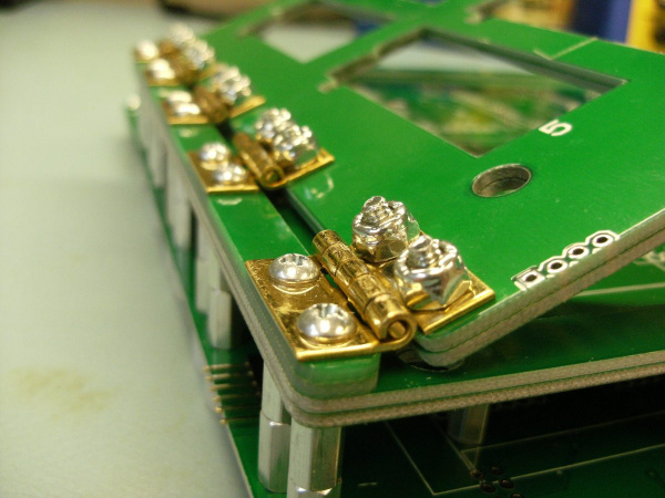
We have also spent a lot of time designing around our gold hinges. It is important to get the spacing and height just right, so that the waffle top comes down nicely on top of the board without any binding. Here is a close up shot of the hinge area of our most recent IOIO testbed:
On this particular design (because it is rather large), we incorporated a few locking header footprints to help with alignment during gluing. We simply put a few header strips through each board and it really helps keep them perfectly aligned while the glue dries.
Shift Registers to Control LEDs
Some of our larger testbeds need to indicated the status of 8-16 boards. The technician needs to see if all of the boards passed or failed. To expand the IO capabilities of our standard testbed micro (the trusty ATMega328), we have augmented our designs with shift registers.
Above, you can see that we have daisey-chained two shift registers together. This way we can use the same 5 pins off of our micro to control up to 16 LEDs.
We like this part (74HC595) for two reasons: (1) it's already in our inventory and (2) the SOIC package is relatively easy to hand solder onto a testbed, and very unlikely to jumper.
One might ask, "Why not use a larger micro?" Well, we like to keep things simple, and so that means keeping our desings small, similar, and repeatable. And so we want to keep using the ATMega328 whenever possible. 99% of our testbeds use this micro.
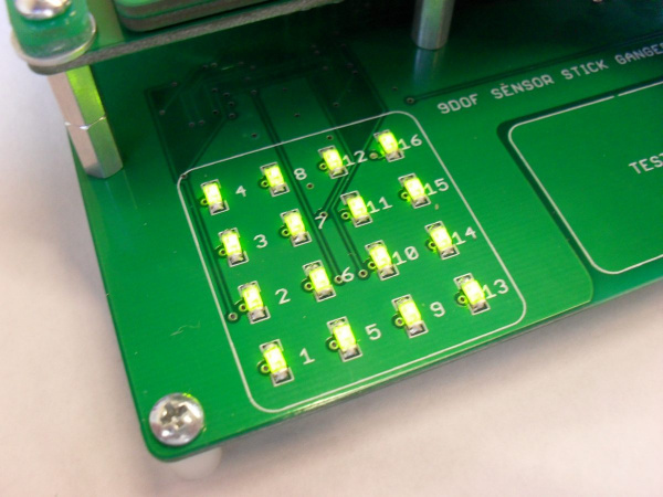
Below is a picture of our multi-board testbed for the 9 Degrees of Freedom - Sensor Stick. Kade Jensen was the test developer on this project, and he appropriately named this the "144 DOF".
Check out all those status LEDs:
All possible thanks to the innovating with a shift register - wahoo!
Cap-Sense Buttons
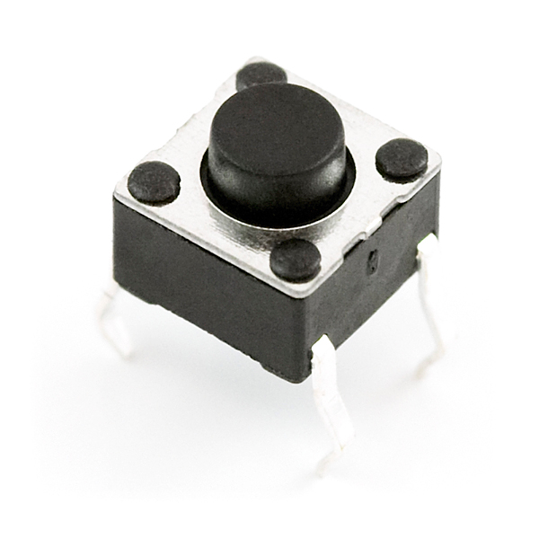
Pictured above is our classic small momentary button. A simple mechanical switch is a great way for the tech to engage a test. We used this button on hundreds of testbeds. There are still hundreds on the production floor today. However, we found that after a few months on the floor (especially with our more popular products that may see 1000s of presses a day), the button would stop working 100% of the time. We found ourselves replacing quite a few buttons each week.
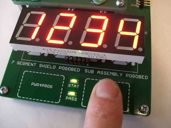
In order to solve this problem once and for all, we moved to a non-mechanical approach: capacitive touch. With this new approach, there is no mechanical connection to wear out, and we never see these fail on the floor. Below is a picture of our testbed for the OpenSegment Shield. You can see the two capsense buttons that engage the different portions of the test.
If you're new to capacitive touch, check out this great tutorial on Arduino here . This is the same library and hardware technique that we use on all of our testbeds these days.
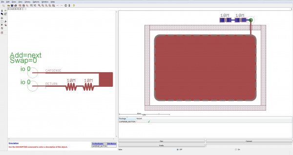
We have also created a special Eagle device that includes a few nice features in the package to speed up design work. It has a good sized metal pad to use as the sense area. It includes no tstop on the pad to protect from finger oils and oxidization. It also has a box of trestrict built into the package to keep the ground pour away. It has a dotted line on the silk to designate the touch area of the button. And lastly, the resistor is built into the package, so this makes it really easy to drop into a design.
At first, we thought that for the more simple testbeds it seemed a bit over-kill to include a micro just to engage a button. But we are finding now that 30 minutes invested in the design and assembly of a testbed is well worth the effort if it can ensure that the testbed will live on for years without the need for repairs. In most cases with QC related hardware, we invest our time and efforts to find the more permanent fix.
The High Side Switch
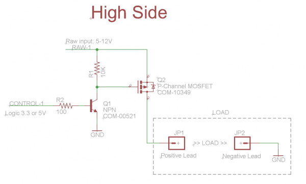
In order to more safely control the power to a board under test, we now use something called a high side switch. This improvement to our testbeds allows us to actively control the power we supply to a board.
Before this innovation, the pogopins on the testbed were always supplying power. We will sometimes call this a "hot" pogopin. Also, the act of swapping out boards on a testbed with this kind of hardware is called "hot swapping". This method of supplying power to the board under test is usually okay for really low power products, and there are still a large number of testbeds on our production floor that have hot pins. However, when you are dealing with higher current devices, it can become rather dangerous.
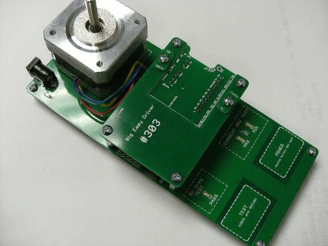
The first product that received this upgrade was the Big Easy Driver. This board, like most stepper motor drivers, requires a substantial amount of current. The original testbed had hot pogopins and so would sometimes lead to damaging the board under test and/or the testbed itself.
Unfortunately, I was unable to dig up a decent picture of the original testing hardware. But I was able to get the most recent version:
Notice how there are cap-sense buttons for the technician to engage the test. When he or she presses this button, it will first turn on the high side switch (powering the board under test) and then engage the test. This ensures that the tech does not press a board down on hot pogopins.
Another issue that occurs with hot swapping is the possibility of momentary, accidental shorts. When a technician places a board down onto a testbed, sometimes they may accidentally slide the board horizontally. If VCC and GND are positioned next to each other on the board design (which often is the case), then this can cause a short between them for a small instance. This can cause large spikes in current and be damaging to the board and testbed. Using a high side switch helps avoid the possibility of these accidental shorts.
The circuit of a high side switch is actually quite similar to our MOSFET Power Control Kit. Below is a schematic view of our high side switch template:
Pre-Testing for Jumpers
In July of 2013, we changed from testing the IOIO OTG with a raw input power of 9V up to 15V. This was to ensure that the board would work for our users at even larger input voltages.
This also lead to killing a lot of our testbeds. We eventually found that if there was a short to ground on any of the power rails (on the IOIO board under test), it would usually fry the testbed and the board. Our immediate fix was to have our technicians use a multimeter to check for shorts to ground on all of the power rails. Although this enabled us to continue building and testing IOIOs, it was not the most efficient way to pre-test. We knew there must be some way to automate this pre-test.
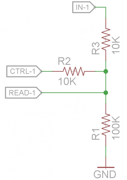
So, one afternoon, I told Pete Dokter about our troubles, and he helped us come up with the following test. It basically uses a voltage divider to measure a line and see if it has a jumper to GND.
It requires two pins from your micro: a control pin (digital) and a read pin (ADC). By manipulating the control pin HIGH and LOW, and watching the voltage on the read pin, we can know if the input pin (the power rail in the case of the IOIO) is jumpered to GND.
If the IN-1 net is grounded, then the READ net should sit at roughly 1/2 of CTRL-1 (logic level). Combined with the power control of a high side switch, this allows us to avoid powering up a board that has a jumper to GND, and ultimately saving the board-under-test and the testbed from potential damage.
Here is the function we use to test for jumpers on the latest IOIO testbed:
language:c
boolean jumper_test(int control_pin, int read_pin){

  digitalWrite(pre_testing_led, HIGH);

  pinMode(control_pin, OUTPUT);
  pinMode(read_pin, INPUT);

  digitalWrite(control_pin, HIGH);
  delay(200);
  int reading = analogRead(read_pin);

  if(debug){
  Serial.begin(9600);
  Serial.print("\t reading:");
  Serial.print(reading);
  Serial.end();
  }

  pinMode(control_pin, INPUT);

  int jumper_val = 486;

  digitalWrite(pre_testing_led, LOW);

  if((reading < (jumper_val*1.05)) && (reading > (jumper_val*0.95))) return true; // jumper detected!!
  else return false;

}
We have always put PTC resetable fuses on our testbeds to prevent damage when current spikes, but adding this pre-test is a great way to ensure that the current never surges in the first place. This issue had never come up on previous tests because most of our products require very little current. This means that when we test a board, we can limit our power supplies current (most of our tests call for 200mA). The IOIOs, on the other hand, require much higher current for testing the charge circuit. They actually draw up to 800 mA when charging our tablets.
Although it was kind of painful to see so many testbeds bite the dust, it was ultimately a good thing because it pushed us to make even better testbeds. We now have an extra tool to use for high current products!
Pad Size, Fillets, and AOI
As part of our constant quest to improve our testing thoroughness, in the spring of 2011 we purchased our first AOI machine (automated optical inspection). After watching it run a few panels of boards, we quickly named it "Disco Stu". If you've ever seen an AOI machine run, than you probably remember a lot of flashing lights of various colors. It's actually quite a spectacle to watch and usually has a pretty good "Ahhhhhh" effect on tours.
The AOI's primary purpose is to look at boards and tell us if there are any manufacturing errors. It checks for 3 things:
Marks (to tell us if the part is in fact on the board and the polarity is correct)
Solders (to tell us if there is sufficient amounts of solder and how well it reflowed)
Lead banks and Toes (to tell us if any legs on an IC jumpered together and/or do not have sufficient solder on the toe of the leg)
As we programed more recipes (unique to each of our 500+ in house assemblies) we started to notice that the machine was having difficulty inspecting some of our components - particularly our 0603 solder joints. The reason was that the solder joint was forming underneath the component legs. This made it difficult for the top down camera to see. Also, the solder was not forming a fillet on it's edge. In stead, it was basically forming a little bubble below.
There was a trend in our earlier designs to use 0402 sized packages on the PCBs and then populate an 0603 sized part. This was done in an effort to save space, while still using a component size that is moderately easy to handle with a set of tweezers.
We did this for years, and it didn't seem to be that big of a problem. But now, with our new AOI machine, we wanted to fine tune our processes even more and narrow in on any manufacturing errors -- no matter how small they may have been. We wanted to start catching the very rare cases where an 0.1uF capacitor would tomebstone and sneak through production to your workbench.
To understand how this problem was effecting the AOI, we need to look closer at how the machine does it's testing. It actually looks at the same component in a variety of ways under three different colors:
White (all white LEDs pointing straight down on the board)
Red (this is primarily useful to see flat surfaces, because the red light is reflected to the side if the surface is anything but flat)
Red, Green and Blue (which are actually hitting the board from 3 unique angles)
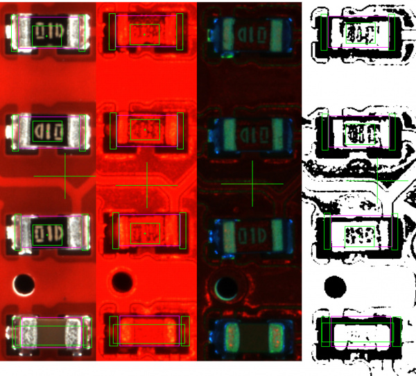
The following graphic is combination of four different images. Each image was taken of the same row of components under a unique lighting. This particular design has 0402 pad sizes with 0603 parts populated.
On the right side, we are also seeing the binary bitmap image that the AOI can generate to help inspect for good solder reflow. The binary bitmap is created from the image taken under red light. The white pixels represent flat spots on the board, and the black pixels represent curved surfaces. In this way, a bare pad (without any solder on it) would reflect the red light and would show up as all white pixels. The software can count the white pixels of a designated area on the board and determine if there is sufficient solder present.
If you look at either side of the components, you can see that there is very little pad space to analyze. Most of it is covered up by the component and the solder. This makes it difficult for the AOI to test for sufficient solder.
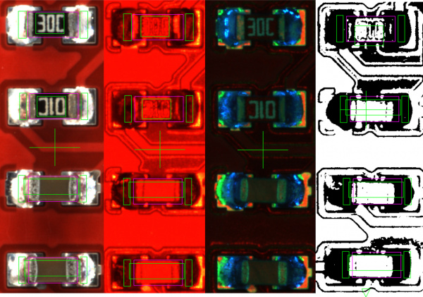
The next image is a similar row of components, but this time they have the correct 0603 sized pads with 0603 parts populated.
Notice how there is more pad visible from this top down view. We can now compare the amount of white and black pixels and verify that there is sufficient solder.
This also helps us determine whether or not the part has slightly tombstoned. When you get a tombstone, the solder left on the pad will usually pillow and have a nice shiny flat spot on the top. The AOI can look for this flat spot under red light and see if the part did not reflow properly.
We have recently made a big push to revise a lot of our older designs to include true 0603 footprints. Each member of our QC team has made an effort to revise at least one design a month (sometimes two!).
Also, all future designs will have the correct pad size. In fact, the production QC team has become very involved whenever designing a new footprint for a new part. We want to ensure that the pad size and shape will promote the best possible solder reflow and that we can utilize our AOI to catch any possible errors.
In an effort to create the best footprint possible, we have recently developed a new technique using images of the bottom side of a component in Eagle. If you like, you can read more about that at our tutorial, Making Custom Footprints in Eagle.
Routing Away and Fake Traces
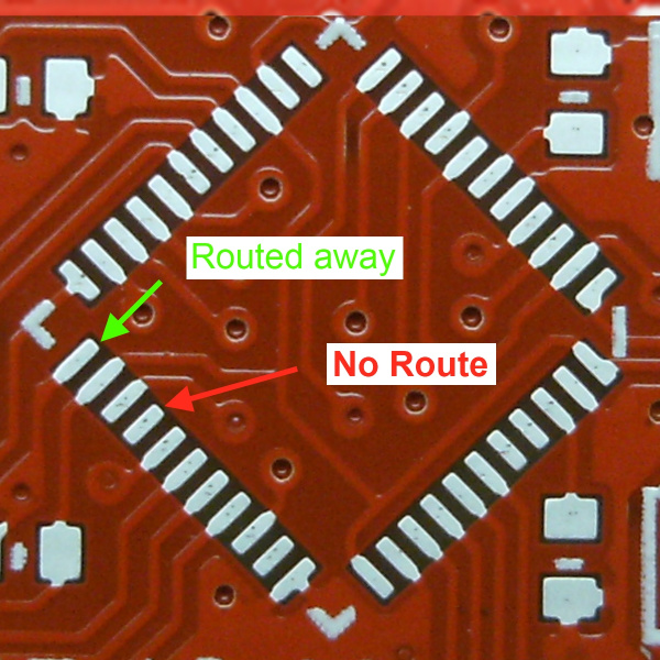
As mentioned in the previous section, we're starting to do a lot more design revisions to help with reflow. One very recent development is the idea of "fake traces". When you route away from an IC (especially small pitched QFN), the route job acctually affects the pad size/shape and ultimately the reflow and fillet formation. Due to the oversized tstop (aka mask cutout) on a PCB, the pad size is actually extended a tiny bit in the direction of the trace. Here is an example:
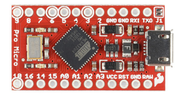
Pictured above is a bare pcb of the Pro Micro. You can see that some of the pads have been routed away from the IC, some have been routed underneath and some pads do not have any routing at all. This slight difference affects the way the solder flows.
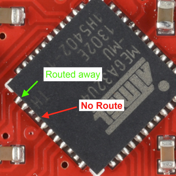
Above is a picture of a populated board. Now let us look a little closer at the left side of the IC.
Notice how the size and shape of the fillet is different for each pad. The pads with the traces routed away look the best! Another added benefit is that the AOI now has almost twice the amount of solder to inspect.
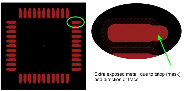
In addition to ensuring that all traces route directly away from the IC, we are also approaching this problem from the library level. In Eagle 6, you can now create complex pad shapes. This means that we can add an extra bit of top copper (in the case below, it is a simple line drawn with the wire tool), and Eagle recognizes the extra copper as part of the pad. In this way, the wire is acting like a fake trace! In the example below, we have modified the pads on a QFN-44 package to include some extra fake traces.
- One thing to keep in mind while doing this: the wire must start on exactly the same X-Y coordinates as the center point of the pad. This is important because it will ensure you do not run into a DRC (design rule check) errors for every pad.
The beauty of this approach is that even if one of the pads is not routed (i.e. its not needed in the design or its a no-connect), it will still have the same shape and padsize-to-paste ratio. The routing direction is now built into the part at the library level - wahoo!!
Resources and Going Further
These are just some of the examples of how we are constantly innovating not only our quality control but our entire board design process. In true open source fashion, we want to share with you every tip, trick, and technique we discover that helps us produce better products. If you have any questions or comments, feel free to hop on over to the discussion section and get a conversation started. Otherwise, check out the next advancements in SparkFun quality control with the Raspberry Pi Stand-Alone Programmer!
Raspberry Pi Stand-Alone Programmer
If you're looking for more information on electronics assembly and design, check out these other tutorials.
