ATmega128RFA1 Dev Board Hookup Guide
This Tutorial is Retired!
This tutorial covers concepts or technologies that are no longer current. It's still here for you to read and enjoy, but may not be as useful as our newest tutorials.
 jimblom
Schematic and Hardware
The development board surrounds the ATmega128RFA1 with all of the supporting circuitry one might need to get up-and-running with the chip.
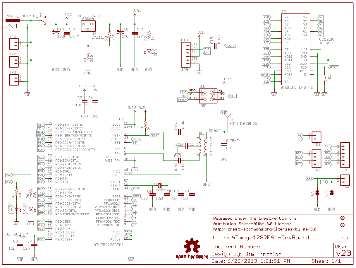
Power Input
The power input section of the circuit includes a voltage regulator, which feeds 3.3V to the rest of the circuit. The following footprints are provided for power input:
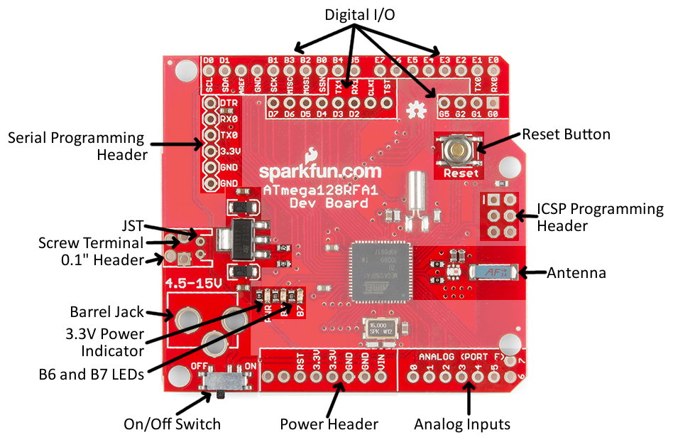
- DC Barrel Jack
- JST connector (2-Pin, Right-Angle)
- 3.5mm 2-Pin Screw Terminal
- Standard 0.1"-spaced header
The slide-switch on the side of the board controls the flow of the input power sources above to the regulator.
The 3.3V and GND pins are also broken out along the side of the board. These nets are unregulated, but can be used to supply a clean, regulated 3.3V voltage source to the board.
ATmega128RFA1 Circuitry
The ATmega128RFA1 is supported by a 16MHz crystal and an assortment of decoupling caps. The RF section of the board has a crystal of its own, as well as a chip antenna and circuitry to support the RF interface. Try to avoid placing components near the antenna, as they may interfere with signal strength.
All digital I/O pins of the ATmega128RFA1 are broken out in some form or another. Two on-board LEDs are connected to the MCU's pins B6 and B7. The remaining I/O's are broken out to the outer headers of the board. The eight analog inputs on port F are available in the same place you'd expect to find an Arduino's analog pins. Key digital pins, like the hardware SPI, I2C, and UART pins, are broken out to the same locations found on Arduinos as well.
Programming Headers
There are two programming headers on the board. One 6-pin (2x3) ICSP header, which can be used to program the chip using a standard AVR in-circuit programmer. A 6-pin serial header near the power inputs can also be used to program the chip (assuming the bootloader's still on there); this header should match up to common FTDI headers and cables (just make sure they're the 3.3V variety).
Powering the Board
There are a variety of ways to power the development board. Input jacks are broken out for barrel jack, JST, screw, and 0.1" connectors. Whichever voltage supply you choose to power the board, it should be between 4.5 and 15V. Each of these power sources is fed into the voltage regulator, which drops the voltage down to 3.3V.
If you're using the barrel jack, a 5V or 9V wall-wart is a good choice for power source.
Voltage can be fed directly to the chip, using the headers labeled "3.3V" -- just make sure the voltage doesn't exceed 3.6V. The ATmega128RFA1 can only operate at voltages between 1.8 and 3.6V.
One of the ATmega128RFA1's key features is its low power consumption. Sending or receiving RF data should only require 16 to 18mA of current. Idling, the chip should only require about 1-4.5mA. Each of the output pins can source/sink between 2-8mA.
Check out the datasheet for more electrical specs.