Programming FPGAs: Papilio Pro
This Tutorial is Retired!
This tutorial covers concepts or technologies that are no longer current. It's still here for you to read and enjoy, but may not be as useful as our newest tutorials.
 Toni_K
Code Translation
This section will cover how parts of code learned in the previous section are translated to the hardware of the FPGA. Remember, FPGAs have a finite amount of space for you to create your design. Knowing how code translates to the hardware will help plan for optimization techniques and where to place it on the chip's floor.
I'll take the clock divider provided in the Github example to explain how it translates to the hardware. Knowing how to translate from code to hardware helps you understand what is really going on. Instead of blindly assuming the compiler is doing things right (similar to compiling a C++ program), we will make sure it is translated the way we want/need it to be.
module clk_div(
    input clk_in,
    input rst,
    input ce,
    output clk_out
    );

// Parameters
parameter DELAY=0; // 0 - default

// Wires

// Registers
reg [DELAY:0] clk_buffer;

assign clk_out = clk_buffer[DELAY];

always @(posedge clk_in) begin
    if ( rst ) begin
        clk_buffer <= 0;
    end else begin
        if ( ce == 1)
            clk_buffer <= clk_buffer + 1;
    end
end

endmodule
We'll start from the top and work our way down.
reg [DELAY:0] clk_buffer;
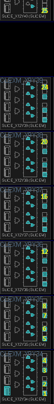
Here, we are instantiating DELAY+1 registers. If DELAY is 24, the code would look like this: reg [24:0] clk_buffer. Since we are counting from 0, we have to count it, and we are actually instantiating 25. In the screenshot below, you can see we have this many created.
assign clk_out = clk_buffer[DELAY]
This line is strictly the MSB bit going to clk_out. This signal is going from the 25th register to a BUFG to distribute to the rest of the design. As seen here:
- The
alwaysblock. This block is where the magic happens. I'll explain the best I can.
Now, we cannot directly associate this block with any one basic element, but we can infer some functionality. We can assume that we will have DELAY+1 size carry logic. (One CARRY4 element contains 4 carry logic elements, which are a MUX and an OR gate).
The clk_buffer <= clk_buffer +1 is pushing data to the registers we defined above, and since this occurs on every clock cycle, we can infer we are sending the data through an inverter. There is no hard coded inverter on the chip, so we are using a LUT for this.
We can see this in the screenshot below.

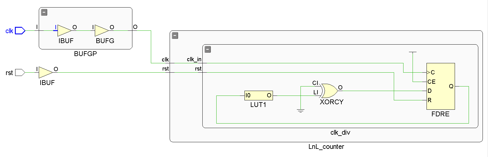
In codespeak, this shows O = !I0.

In laymen terms, this means the input 0 of the LUT will be inverted to the output.
Where is the LUT input coming from? The answer is clk_buffer[0]. This is confusing, because we are actually using the main system clock to drive these registers (posedge clk_in).
On reset (power up) the 25 registers set their initial inputs to 0. From here the clk_in starts to run. After the first clock cycle (positive edge to positive edge), clock_buffer[0] sends its value, which is a 0, to the LUT, which inverts it and sends it to the first carry logic MUX and OR. The OR sends it to clk_buffer[1] and the MUX as a select signal to the next carry logic. It does this 24 more times, and we get to clk_buffer[24]. There, the output goes to a BUFG element where it gets distributed to the rest of the design.
This code will run like this until power is lost.
I invite you to do the same sort of translation for the other modules and see how well you do.