How Does an FPGA Work?
Multiplexers
Now that we have the basic building blocks from transistors to logic gates, we can make something more useful with them. With just logic gates, you can describe any digital circuit. However, there are many reoccurring higher level functions that get their own symbols such as those used for binary math (adders, multipliers, etc).
We are going to look at one of the fundamental building blocks of FPGAs, the multiplexer.
A multiplexer selects a single input out of set based on the value of its select input. Here is its symbol:

The / on the sel line is used to show it is 6 bits wide.
The number of inputs will vary but the multiplexer always just has one output.
The way the select input is encoded will also vary. Usually, you will see it as a binary number, but the simpler circuit uses a one-hot encoding. A one-hot encoding is simply a binary value where there is always exactly one 1. The position of the 1 is the important thing.
A decoder takes a binary value and turns it into a one-hot signal. An encoder turns a one-hot value into a binary number. These can be used to make a one-hot multiplexer accept binary values.
Take a look at how we could implement a one-hot encoded multiplexer using just some AND and OR gates.

If we set the sel value to be 000010, meaning only sel[1] is 1, then we can see that for every AND gate, except for the one with the b input, one of the inputs will be 0. That means that each of those will always output 0 regardless of what the inputs a, c, d, e, and f are. The only input that matters is b. When b is 1, it is AND’d with a 1 and the output of the AND gate is 1. When b is 0, it is AND’d with 1 and the output of the AND gate is 0.
In other words, the output of the AND gate is simply b.
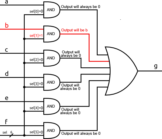
The OR gate in this schematic is shown with more than two inputs. This can be created by creating a tree of two input OR gates where two inputs are OR’d together and the outputs are then OR’d together over and over until you have one output. A multi-input OR gate behaves just as you would expect with the output being 1 if any of the inputs are 1.
However, in this circuit every input to the OR gate is guaranteed to be 0 except the input from the AND gate whose output is b. This means that the OR gate will simply output a 1 when b is 1 and a 0 when b is 0.
In other words, the output of the OR gate is simply b.
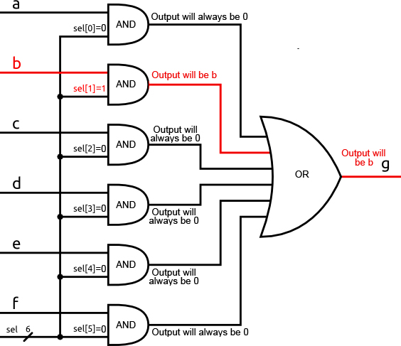
You could repeat this logic for any input and, as long as the input is one-hot, the input that corresponds to the given 1 will be passed through to the output.
You can imagine having a large matrix of multiplexers with a programmable sel input. This would allow you to route signals wherever you needed in your design. This is how FPGAs get their signals where they need to be and it is called the general routing matrix.
Obviously the details for routing thousands and thousands of signals gets messy, but fundamentally it is just using a bunch of multiplexers with select inputs connected to programmable memory.