TXB0104 Level Shifter Hookup Guide
Contributors:
 SFUptownMaker
SFUptownMaker 
TXB0104 BOB Overview
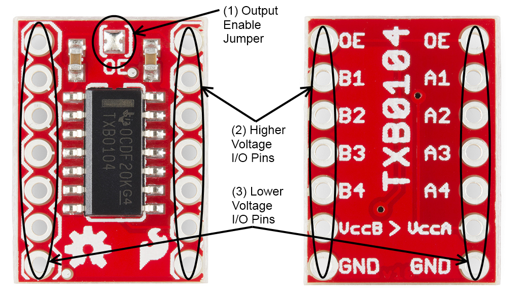
The TXB0104 breakout board is pretty simple. There are two rows of pin headers, one down each side of the board; one side for the high voltage signals and one for the low voltage signals.
- The output enable jumper (1) is closed by default, causing the signals on both sides to be driven at all times. It's up to the user to ensure (as is usually the case) that the system avoid bus contention states where the high side and low side of the same signal are being driven to opposite levels.
- B-side signals (2) are the high voltage signals. VccB must be at a higher voltage than VccA to avoid total protonic reversal (or at least, to avoid possible damage to the chip). The voltage range for VccB is 1.65 to 5.5V. If driving the OE pin from the high-voltage device, please insert a 1k resistor in series with the drive signal.
- A-side signals (3) are the low voltage signals. VccA must be at a lower voltage than VccB. The voltage range for VccA is 1.2V to 3.6V.