THAT InGenius and OutSmarts Breakout Hookup Guide
 Byron J.
Introduction
The THAT 1206 and 1646 breakout boards offer an easy solution to adding balanced audio inputs and outputs to your circuits.
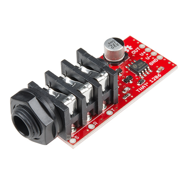
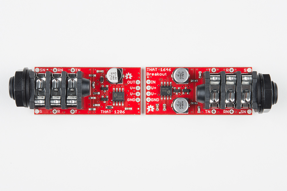
SparkFun THAT 1206 InGenius Breakout
BOB-14002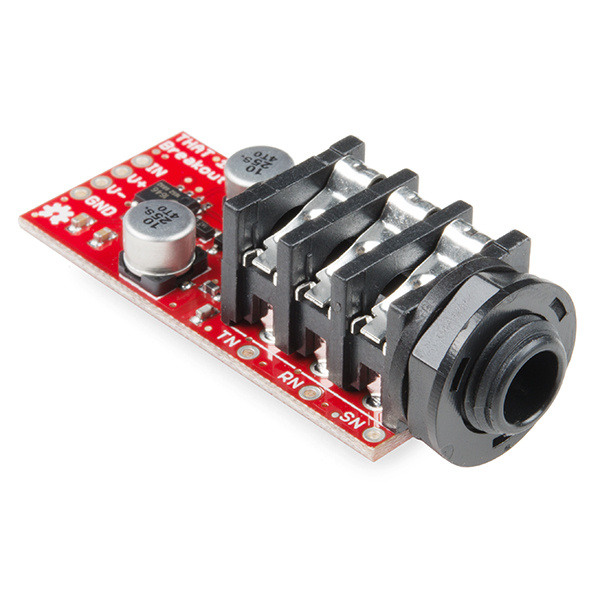
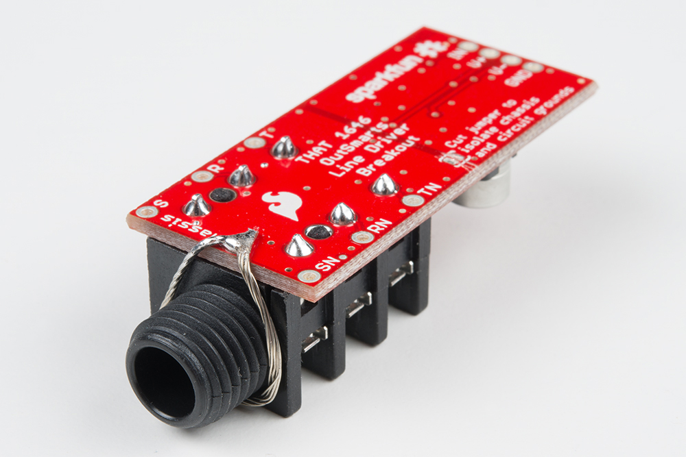
SparkFun THAT 1646 OutSmarts Breakout
BOB-14003The THAT InGenius and OutSmarts technologies are designed for high grade analog audio transmission and reception. They offer low distortion and high common mode rejection in real-world audio applications.
The breakout boards combine the THAT IC, supporting components, and a 1/4" TRS socket. They make it easy to use the input and output drivers on breadboards and in projects.
Required Materials
To follow along with this project tutorial, you will need the following materials:
Tools
For the breadboard exercises, we used the following tools and test equipment.
- A signal generator.
- A biploar power supply. We used two different supplies.
- For bench testing, we're using an old HP 6205c adjustable supply.
- We also used a MeanWell +/-15V supply.
- An oscilloscope to observe the results
Suggested Reading
If you aren't familiar with the following concepts, we recommend checking out these tutorials before continuing.
Analog to Digital Conversion
How to Use a Breadboard
Analog vs. Digital
Background
Before we look more closely at the THAT breakout boards, let's explore what they're used for: driving and receiving differential (AKA balanced or double-ended) signals.
Signaling Model
A typical model for analog electronic commmunication involves a transmitting device, which sends signals to a receiving device. In between, they're connected with a conductor: traces on the printed circuit board, or wire between the devices.

In a simplistic approach to analog signaling, the transmitter simply puts voltage on the line, and the receiver observes that voltage.

Sometimes, the connection runs through a less-than-ideal electronic environment. It could pick up additional unwanted voltage from sources along it's path. In signaling theory, unwanted signals are known as noise. Sources of noise could include digital signals on the same PCB, or nearby radio or electromagnetic equipment.

In these cases, the receiver receives the combination of the original signal, plus the noise picked up along the way.
Differential Signals
Differential signals use a bit of clever algebra to achieve noise cancellation.
The output generates two signals, one in original polarity (known as the hot leg), the other inverted (the cold leg).

The receiver subtracts them from each other, to restore the original signal.

Any noise picked up along the way will be the same on both signals. When they're subtracted, the inverse polarity signal is reinforced, but the noise is canceled! N - N = 0!

Differential signaling takes advantage of the principle of common mode rejection. When the signals are subtracted, anything that they have in common gets canceled. The degree of common mode rejection achieved is typically expressed in decibels, known as the common mode rejection ratio, abbreviated CMRR.
The Difference between Differential and Balanced?
In this hookup guide, we're specifically talking about the analog audio application of differential signaling. In audio literature, this is usually referred to as balanced interfacing. It's a problem-domain specific term, used to describe the more general principle of differential signaling.
Differential signaling is not limited to audio or analog interfacing. A modern computer is full of differential digital interfaces: USB, LVDS RAM, displayport, and SATA all use variants of differential digital signals.
Balanced Signals In Audio Systems
Any audio system involves devices that employ a wide number of connectors and signaling standards. To properly connect everything, you need not only an understanding of the different connectors being used, but also the circuits behind them! The following table summarizes some of the possibilities.
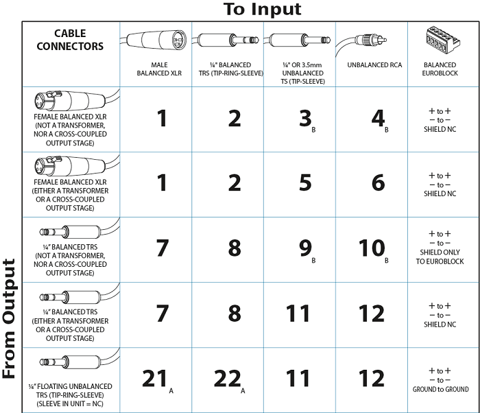
There are some particular pitfalls what await in the audio interfacing world.
- 1/4" TS and TRS sockets look the same from outside, but aren't functionally equivalent.
- TRS jacks are used for balanced outputs, headphone connectors, and insert-point connections. The connector is the same, but they're not compatible with each other.
- There's no guarantee that an XLR is actually balanced. There have been devices that left a pin disconnected!
- There was also a period of disagreement as to which pin on an XLR was hot. Today things have mostly settled on pin 2 being hot, but if you're having problems, you might have a pin-3 hot device.
- No matter how carefully selected the equipment is, Murphy's Law dictates there will be one essential piece of unbalanced equipment.
With some equipment, you're lucky, and the interfacing details are printed near the connector in question. Other times, they're described in the users manual, and sometimes you're left to figure it out on your own!
Sometimes, just using the right combination of connectors or adapters gets things into decent shape. Other times, it might be easier to modify or retrofit a better input or output stage...
Hardware Overview
The THAT InGenius and OutSmarts integrated circuit families implement high quality balanced input and output amplifiers with a minimum of external components. The circuit topologies were invented by Bill Whitlock, the President and Chief Engineer of Jensen Transformers. Mr. Whitlock is also a recognized expert on audio interfacing, having published many papers and troubleshooting guides on the subject. They are manufactured by THAT Semiconductor, who specialize in high-quality analog audio ICs.
These two breakouts perform mirror-image signal conversion. The 1646 OutSmarts is a unbalanced-to-balanced output driver, and the 1206 InGenius is a balanced-to-unbalanced input receiver.

The breakout boards add passive components to support each IC, plus TRS jacks.
The circuits come from the THAT datasheets, and include the recommended RF filtering, DC offset reduction, and transient suppression networks.
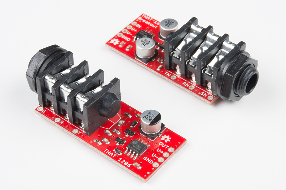
THAT Breakout Boards
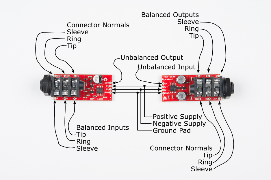
The external interface on each board (the output of the 1646 and the input of the 1206) is on a 1/4" TRS socket. The TRS is wired with the regular-polarity signal on the Tip, and the inverted signal on the Ring. Adjacent to each leg of the socket are test points for the signal (T, R, S) and normal (TN, RN, SN) contacts. When nothing is plugged into the socket, the normals connect to the corresponding signal pad. When a jack is plugged in, it connects to the signal pads, and the normals float.
The internal connections are on four 0.1" header pads.
| Pad Label | Function |
|---|---|
| In | 1646 unbalanced input |
| Out | 1206 unbalanced output |
| V+ | Positive power supply rail |
| V- | Negative power supply rail |
| GND | Ground |
Grounding
There is a jumper on the back of the PCB that allows for two different grounding configurations.
By default, the board assumes a single ground connection through the 0.1" header. This is how you'd deploy these breakouts on a breadboard, or in a plastic enclosure.
However, if you have a grounded metal enclosure, it's considered bad practice to run the shield of the cable around inside the Faraday cage of the enclosure -- it creates an antenna within the cage that re-radiates any noise induced in the shield.
The solution to this is to tie the shield to the enclosure right at the connector. On these breakouts, there is a jumper to separate the connector from the circuit ground, and pads that allow for a short ground wire to run under the collar of the TRS.
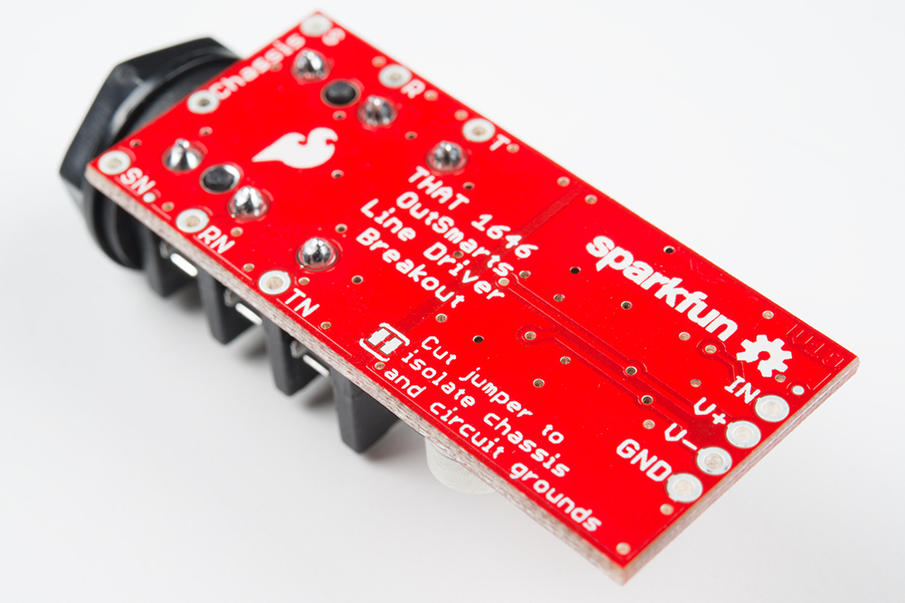
We'll examine how these are applied in the example project below.
Power and Headroom
Before we build some circuits with the THAT breakouts, let's discuss how to power them, and what that means for headroom.
Analog audio circuits usually run from bipolar power supplies, meaning the supply provides two rails, of equal and opposite voltages. The THAT breakouts follow this convention, and function across a wide range of supply voltages, from +/-5V, to an absolute maximum of +/-20V.
The power supply voltage determines how large a signal the IC can handle before clipping: for the THAT ICs, the clipping voltage is roughly 2 V below the supply rails. For example, running on +/- 12V rails, the ICs can handle 20 Vpeak-to-peak signals, which swing between -10V and 10V. If the signal exceeds that range, it will clip, resulting in distortion.
As the supply voltage changes, the point at which the IC clips move correspondingly. Typical pro-audio devices run on +/-15V to +/-17V supplies, while consumer hi-fi devices frequently have +/- 12V supply rails.
Finally, there is a bit of cleverness at play with the maximum signal levels from these ICs. The 6 in the name of each IC refers to how much gain or attenuation is applied to the signals they pass: 6 dB. The 1646 drives each leg of the balanced output with a signal that is as strong as the input -- the differential voltage is double the input voltage, or 6 dB hotter. The 1206 does the reverse: it cuts the input voltages in half (-6 dB) -- its unbalanced output is the same amplitude as either of the input legs.
If you daisychain a 1646 into a 1206, the output of the 1206 will be equal to the input to the 1646.
Breadboard Experiments
To get started with these boards, lets build a few circuits on a breadboard, and observe their performance on an oscilloscope. You'll need the materials listed above, in the required materials section.
You'll also need a bipolar power supply, signal generator, and an oscilloscope to follow along.
Balanced Output With 1646
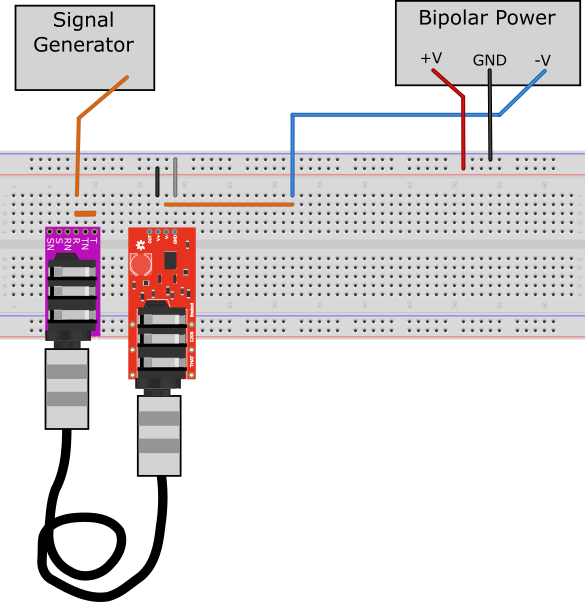
First, we'll convert the unbalanced output of our signal generator into a balanced output, using the 1646 breakout.
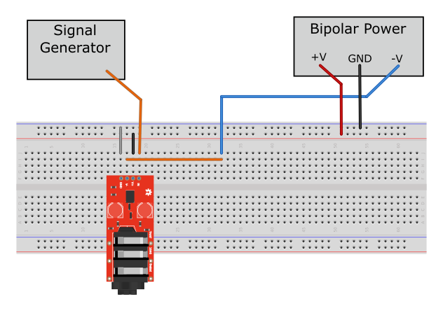
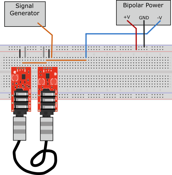
We assembled the circuit on a solderless breadboard. Because we're using a bipolar power supply, we had to run three wires (V+, ground and V-) from the power supply. We also connected the output of our signal generator to the input of the breakout.
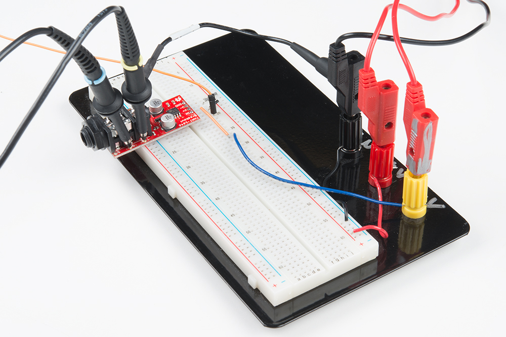
With the generator, adjustable power supply, and oscilloscope, we can evaluate the behavior of the 1646.
Set the signal generator to produce a 1 kHz sine wave at 5 Vpp, and set the power rails to +/- 12V. Then switch the power supply on, and use the oscilloscope to observe the signals at various points in the circuit, as discussed below:
- The breakout draws about 5 mA from each supply rail. If the draw is higher than that, switch the supply off and double check your wiring.
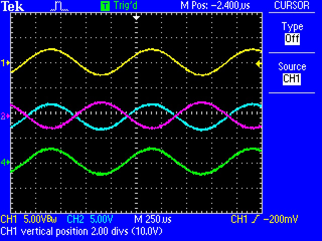
- Probe the signal generator output and Tip of the TRS connector: the signal polarity and amplitude are identical.
- Compare Tip and Ring outputs: they should be same amplitude, but with opposite polarity.
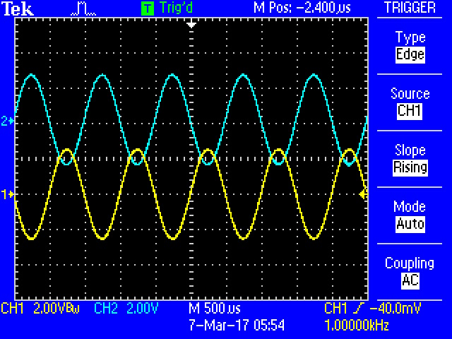
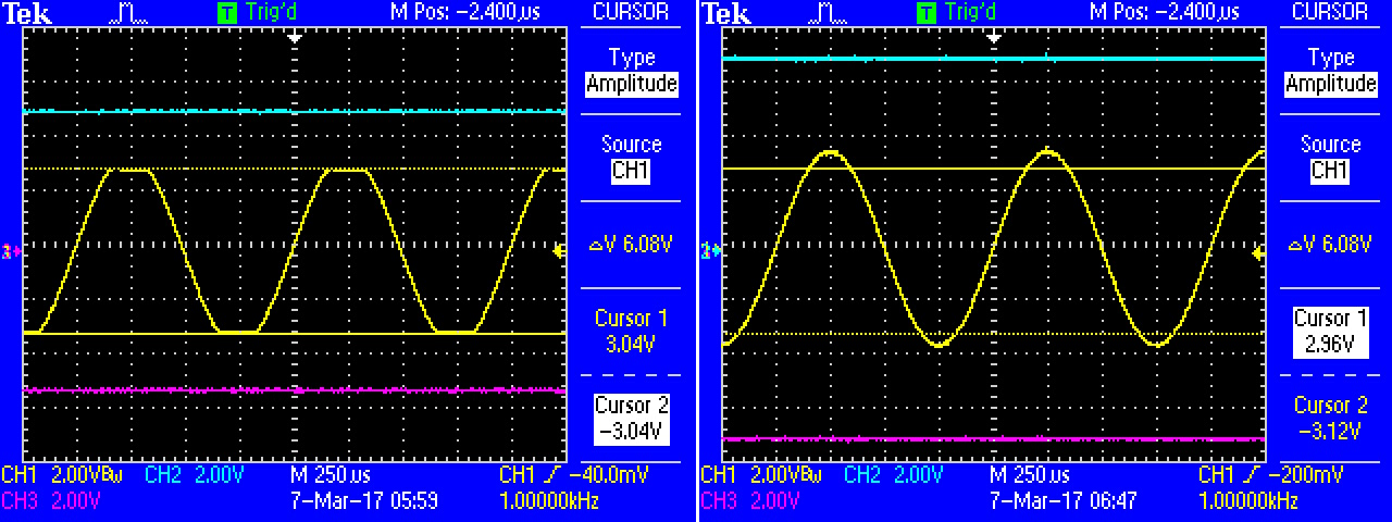
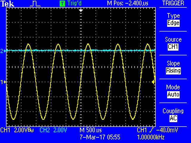
- Keeping the probes on the Tip and Ring outputs, short the ring connection to ground (we used a snip of wire to bridge the ring to the sleeve). The voltage observed at the tip doubles to 10 Vpp, and the ring goes to 0V. The 1646 keeps the differential amplitude the same (10V - 0V is equivalent to (5V - (-5V)) ), and the 1646 still exhibits 6dB gain. The supply current remains at 5 mA per rail.
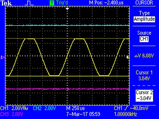
- Finally, let's check the clipping amplitude of the 1646. Reduce the supply rails to +/- 5V, then increase the generator amplitude while monitoring the output signal. The output will start to clip when the generator reaches 6 Vpp. Once you see the clipping, increase the supply rails slightly, and notice that the clipping point tracks the rails.
Balanced Input With 1206.
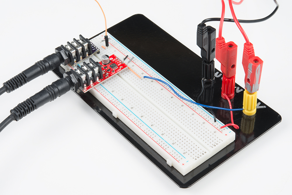
Moving on, we'll add a 1206 breakout to the circuit we built above.
We plugged them together with a TRS cable.

Checking the behavior of the circuit with the oscilloscope, we observe:
The 1206
OUTpin matches the original input.
- As with the previous experiment, shorting one leg of the interconnection to ground results in no change to received amplitude.
Common Mode Rejection Test
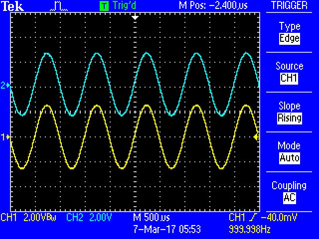
As illustrated in Figure 5 of the 1206 datasheet, we can test common mode rejection by applying the same output from a signal generator to the Tip and Ring of the 1206 input connector, and observe the output with an oscilloscope.
To make the connection a little easier, we used a TRS breakout board, and connected it's T and R pads with a wire on the breadboard. Then we ran a TRS cable from the TRS breakout to the THAT 1206 board.
Set the signal generator for a 1 kHz sine wave, and slowly increase the signal generator amplitude, while keeping an eye on the board output. The output will be extremely small when compared to the input. On our test system, we applied 5 Vpp and could not measure any significant signal at the output -- the scope's finest input range is 20 mV per division. THAT state the 1206's CMRR as better than 90 dB, which translates an algebraic factor of about 32,000.
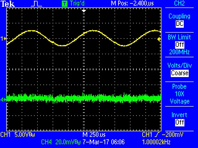
Notice that the output scale is 20 mV per division.
By adjusting the generator frequency, we can observe that the CMRR is similar across the audio spectrum, from 20 Hz to 20 kHz.
Example Application
Next, let's take our newfound skills with these breakouts, and use them to retrofit balanced outputs onto a device that doesn't have them already.
The candidate device is a Sony hi-fi component CD player. From the factory, it only had RCA jack outputs, but we're going to augment them with balanced TRS outputs, using a pair of THAT 1646 OutSmarts breakout boards.
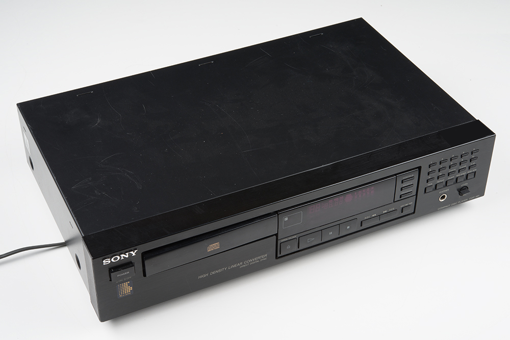
This particular unit was selected for a couple of specific reasons.
- First, it was working to begin with -- it's easier to add a feature to something that's already working, than to have to start with troubleshooting and repair work.
- Second, as a stereo component, it's in a reasonably large chassis, with plenty of room inside for the added components. There simply wouldn't be room inside for more components in a Discman-style portable player.
- Finally, it's a little older -- there's a sticker on the back panel indicating it was manufactured in 1991. That means that the components inside larger and less highly integrated, making it a little easier to accomplish the retrofit.
First step: Analysis
To add the THAT 1646 breakouts to this player, we needed to know several things:
- First, we need to find a place to mount them, where they won't cause problems with the inner workings of the player.
- Second, we need to identify the power supply rails in the player, and figure out how to power the breakouts. We're operating under the assumption that there will be a bipolar power supply that we can tap into.
- Finally, we need to figure out where we can tap the audio outputs, and verify that the signal we're extracting meets the 1646's allowable headroom levels
Mechanical Analysis
Finding a place to mount the breakouts was as simple as undoing the four screws to remove the top of the player. With the top off, it's apparent that the chassis is mostly empty space, and there's plenty of room for added circuitry.
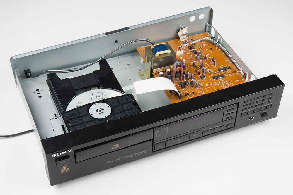
We opted to mount the breakouts to the back panel, next to the existing RCA jacks. The breakouts will be mounted using the nuts on the TRS jacks.
Power Supply Analysis
We then needed to figure out how to power the breakouts. We know each board draws about 5 mA from each power supply rail, and can function on supplies from +/-5 to +/- 20 VDC.
Looking in the player, there are a number of labeled wire jumpers on the PCB. In particular, there were jumpers labeled +5V, -5V, +10V, -10V and GND. +/- 10V sounds like a good starting point for the 1646, leaving plenty of headroom, but more careful inspection contradicted that thinking!
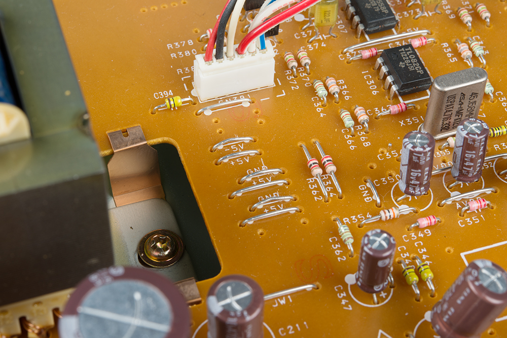
Just inside the RCA jack are the player's output stages, a pair of TL082 op amps, which were powered from the +/- 5V rails. A little more careful inspection with the oscilloscope revealed what was going on. The 10V lines are the raw output from the bridge rectifiers, and exhibit 60 Hz ripple. The 5V lines are the output of an M5209P voltage regulator, with no visible ripple.
Signal and Headroom Analysis
It was easy to find the output signals. Near the RCA jacks are a pair of wire jumpers, clearly labeled L and R. Those jumpers measure continuous with the tips of the RCA jacks.
To evaluate the headroom required, we burned a CDr with full amplitude sine wave test signals. Playing those tracks resulted in output amplitude of 5.6 Vpp, and we verified this as several frequencies across the audio spectrum.
The 5.6 Vpp level just happens to dovetail with the headroom that we measured on the breadboard. Powered from +/- 5V, the 1646 can handle input signals up 6 Vpp.
Putting It All Together
Materials
Aside from the CD player, we needed the 1646 breakout boards and some hookup wire.
We also used a drill press with a set of graduated metal bits, cutting oil, and soldering tools including an iron and wire strippers.
Mounting The Breakouts
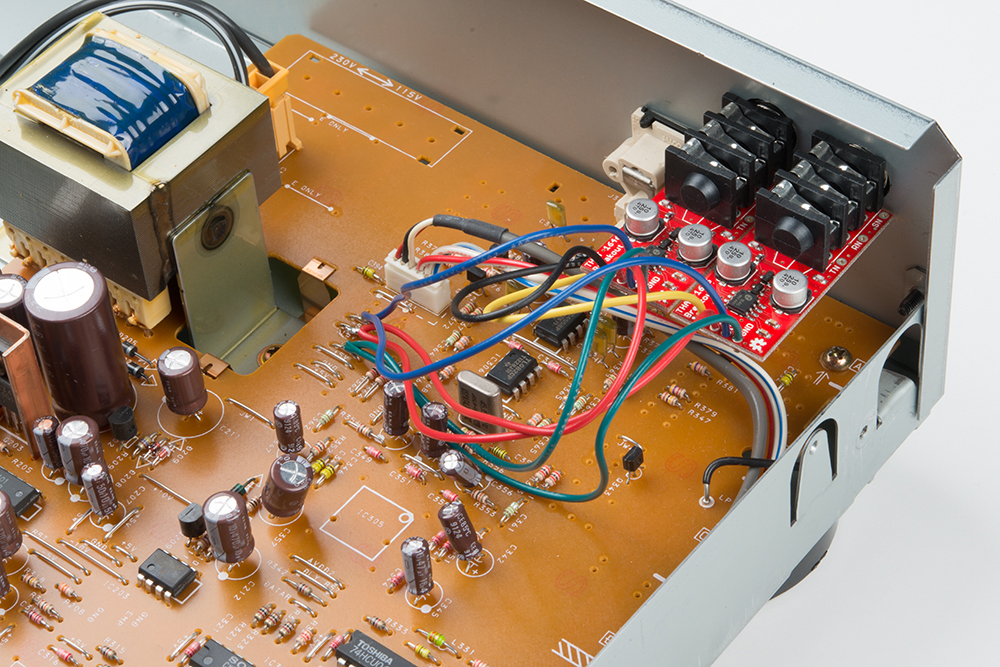
The rear panel comes completely off the back of the unit, which allowed us to drill holes to mount the breakouts without being concerned about metal chips falling into the rest of the unit. Since the panel and chassis are metal, we cut the shield jumper on the bottom of the board, and soldered a loop of stranded hookup wire to the ground pad.
When the breakout is mounted in the panel, the loop makes contact with the chassis.

We then ran some short pieces of stranded wire to the points identified in the analysis. The wiring went like this:
| Wire color | Connection in CD player | Point on breakouts |
|---|---|---|
| Red | +5V | V+ (both boards) |
| Green | GND | GND (both boards) |
| Blue | -5V | V- (both boards) |
| Yellow | L | IN (Left board) |
| Black | R | IN (Right board) |
Each board got it's own power wires; the far ends of those wires were twisted together, and tack soldered to the corresponding points on the CD player board.
With everything assembled, it's time to test it out, then close the player back up!
Resources and Going Further
Now that you've successfully got your THAT 1206 and 1646 up and running, it's time to incorporate them into your own project!
Resources
For more information about the THAT InGenius and OutSmarts ICs, please refer to the datasheets and application notes below.
- THAT 1646 Datasheet
- THAT 1206 Datasheet
- Bill Whitlock's AES paper introducing the THAT 1200 family.
Going Further
For more information about balanced audio and sound system design, please refer to the following materials.
- Bill Whitlock is one of the leading experts on the subject of designing balanced audio interfaces. He has written many papers on the subject, including:
- Douglas Self's Small Signal Audio Design book is a great guide to audio circuitry in general.
- Norman Crowhurst's book of Audio Measurements explains how to quantify audio parameters such as frequency response, CMRR, and distortion.
- Discussion of the pin 1 problem
- Rane Application Note 110 is a very useful resource discussing the connection of balanced and unbalanced audio gear. Their App Note Library contains a number of other useful resources.
Need some inspiration for your next project? Check out some of these related tutorials: