Introduction to Operational Amplifiers with LTSpice
 LightningHawk
The Ideal Op Amp
The op amp is designed to detect the difference in voltage applied at the input (the plus (v2) and the minus (v1) terminals, or pins 2 and 3 of the op amp package). The difference is also known as the differential input voltage. The output, then, is the difference sensed at the input multiplied by some value A - the open-loop gain. An op amp behaves as a voltage-controlled voltage source, which we will model now. We will simulate both an open-loop and a closed-loop amplifier configuration.
An ideal op amp has the following characteristics:
- Infinite open-loop gain
- Infinite input resistance
- Zero output resistance
- Zero common-mode gain = infinite common mode-rejection
- Infinite bandwidth
- Zero noise
- Zero input offset
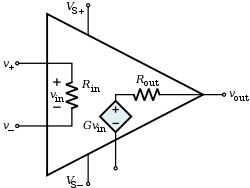
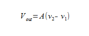
Because the input resistance (Rin) is infinite, we can deduce that the current seen at the (+)(v2) and (-)(v1) terminals are zero, using Kirchhoff's laws. Since the output resistance (Rout) is zero, there is no voltage loss at the output. The diamond-shaped voltage source in the image above is known as voltage-dependent voltage source, and in this case the voltage is the gain (G) multiplied by the difference between the input terminals (Vin). The gain is normally referred to as (A) in texts, so the equation for the output is given by:
Let's model a voltage-controlled voltage source and see if we can't get its behavior to mimic an ideal op amp.