External IO and Metastability
Constraint Files
Constraint files are used to specify specific design constraints that are FPGA specific. There isn’t a current standard for the use of these as each FPGA manufacturer wants to allow different features.
Pin Locations
The most common use for these files is constraining a top-level input or output to a physical pin and to make this easy, Alchitry Labs supports Alchitry Constraint Files or ACFs. These have a very simple syntax and will work for either the Au or Cu.
If you create a new project for either board, under the Constraints header in the project navigator you’ll find a file called alchitry.acf. This file contains the basic pinout definitions for the board. This is the Alchitry Constraint File for the project we created in the Alchitry PWM tutorial.
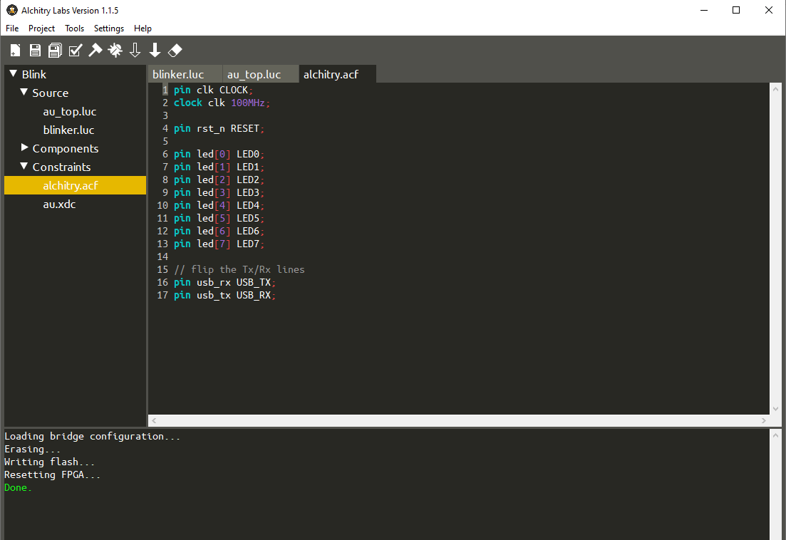
Looking closer at this file, you'll see the following (or something very similar):
pin clk CLOCK;
clock clk 100MHz;

pin rst_n RESET;

pin led[0] LED0;
pin led[1] LED1;
pin led[2] LED2;
pin led[3] LED3;
pin led[4] LED4;
pin led[5] LED5;
pin led[6] LED6;
pin led[7] LED7;

// flip the Tx/Rx lines
pin usb_rx USB_TX;
pin usb_tx USB_RX;
The syntax for a pin location definition is pin signal PIN; where signal is the name of the input or output in your top-level module and PIN is the physical pin to connect it to. You can also put the optional pullup or pulldown keyword after the pin name but before the semicolon to specify if the on-chip pullup or pulldown resistor should be enabled. These are only for inputs. Also note that the Cu doesn’t support pulldowns and the keyword will be ignored.
Alchitry Labs defines some special pin names for the signals on the board such as RESET and LED0. These are useful since they map to different physical pins on the Au and Cu but the tools know which pin to use.
All the broken out IO pins also have convenient names using the format of the bank letter followed by the pin number.
The pinout of the Br Element looks like this.
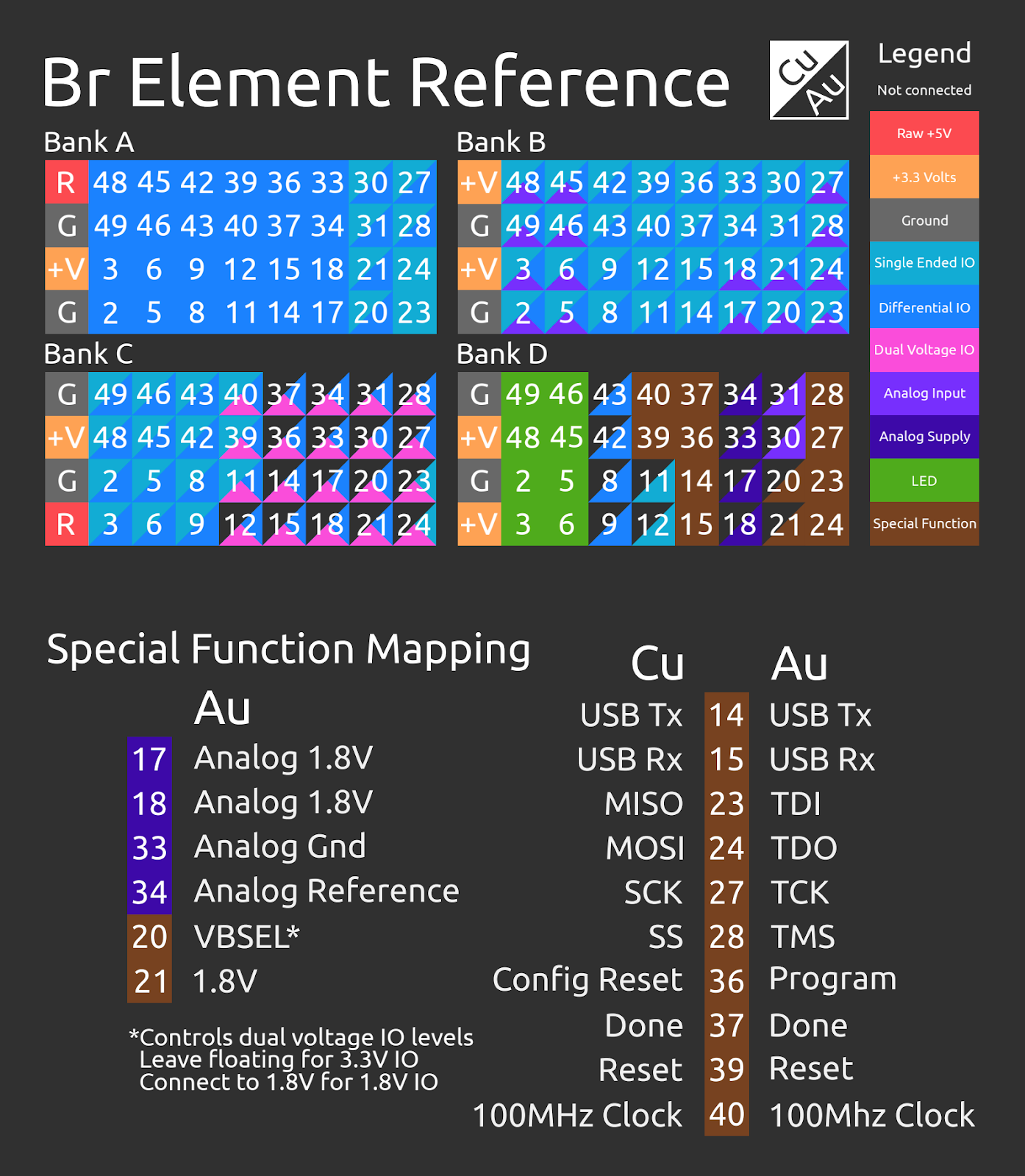
Bank A is the top left connector when looking at the board with the USB port on the left. Bank D is the bottom right. Basically, the same layout as the reference sheet.
If you want to use, say, pin 2 of bank A, you would use the pin name A2. This name is the same regardless if you are using the Au or Cu. These names then get mapped to the physical pin of the FPGA chip by the tools.
The top left corner of each square corresponds to the Cu’s pin’s capabilities and the bottom right half is the Au’s. These halves are sometimes split again if there are multiple uses for a pin.
For example, pin A20 can be used as a differential signal with the Au but only as a single ended signal on the Cu. Pin B2 can be an analog input or a differential signal on the Au but only a single ended signal on the Cu.
Also note that all differential IO can be used as single ended IO as well.
Banks A and B are fully loaded on the Au and Cu while bank C is only partially loaded on the Cu and bank D is mostly special signals.
The second half of the reference sheet is the signal mapping for bank D. For example, D14 is the USB Tx signal on both the Au and Cu.
All the analog signals and dual-voltage select signals are only on the Au and aren’t connected to anything on the Cu (noted by the black top left of the square).
Clock Definitions
When you have a clock input in your design, you need to tell the tools how fast the clock runs. This can be done in the Alchitry Constraint File as well using the clock signal frequency; syntax.
For the clock built onto the board, clock clk 100MHz; is used to specify that it is 100MHz.
This is important so that the tools know how fast your design needs to run. Without this, they don’t know what timing requirements to meet when laying out your design.
Other Constraint Formats
If you want to specify more advanced constraints, you can add Xilinx or Lattice specific constraint files to your projects for the Au or Cu respectively.
If you make an Au project, you’ll actually already have a Xilinx Design Constraint file called au.xdc in your project. This file has information telling the tools what voltages are used, and some info about the flash holding the FPGA’s configuration.
If you want to really dive into it, you can read Xilinx’s documentation here or click on the button below.
Typically, you will never have to mess with these unless you start doing some really advanced stuff.
Lattice’s constraints are split into PCF and SDC files. PCF stands for physical constraint file and is used to define the pinout and SDC stands for clock design constraint is used to define the clock frequencies.
Refer to the iCEcube2UserGuide - specifically chapters 5 and 6 - for more details.
Again, you shouldn’t need to write these yourself if you are using Alchitry constraints.