If you're like me and you've decided to take the plunge from EAGLE PCB to KiCad it can be really jarring. EAGLE had many quirks and rough edges that I'm sure I cursed when I first learned it back in 2005. Since then EAGLE has become a second language to me and I've forgotten all the hard bits. So as you migrate to KiCad remember to take breaks and breathe (and say 'Key-CAD' in your head). You'll be dreaming in KiCad in no time!
This tutorial will walk you through a KiCad example project from schematic capture to PCB layout. We'll also touch on library linking, editing, and creation. We'll also export our PCB to gerbers so the board can be fabricated.
While this tutorial is aimed at beginners I am going to use terms such as 'schematic components' and 'polygon pours'. If something doesn't make sense that's ok, just take a moment to do a quick search. If you really get stuck please use the comments section on the right. We always want to improve our tutorials to make them easier.
Note: This tutorial was written using KiCad 4.0.6 on Windows 10. (i.e. Use this version to follow along.)
v5 Workaround: Users attempting to use more up-to-date versions of KiCad will inevitably run into issues following this tutorial, step-by-step. However, one of our customers has graciously provided various workarounds for v5 that may be of interest to others who are pursuing the same route. Check out the comments section for more info.
Users can also check out these other tutorials on KiCad (v5):
Let's get started! Head over to KiCad's download page and download the latest version of the software for your specific platform:
Warning: Make sure the domain is kicad.org when downloading the KiCad software!!! When installing KiCad, please always verify the installation signature. Starting with KiCad version 5.99, all installs are signed by KiCad Services Corporation.
For more information, check out this note from one of the KiCad developers in the KiCad Forums: Warning Avoid All Links to ... or read about it from Hackaday: KiCad Team Releases Warning Regarding Domain Name.
Once installed, run KiCad. A main navigation window will display where you will be able to open all the periphery programs like schematic capture and PCB layout.
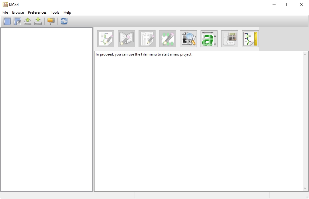
The KiCad project window looks quite empty and sad. Let's open an example!
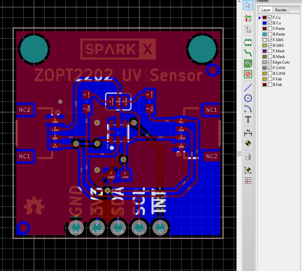
The ZOPT2201 UV sensor designed originally in SparkX is a great I2C UV Index sensor and will serve as our starting example for this tutorial. Download the ZOPT220x UV Sensor Breakout designs for KiCad and unzip the four files into a local directory:
Once the four files are located in a local directory (try looking in your downloads folder for ...\ZOPT220x_UV_Sensor_Breakout-Tutorial), click File -> Open Project and open the ZOPT220x UV Sensor Breakout.pro file.
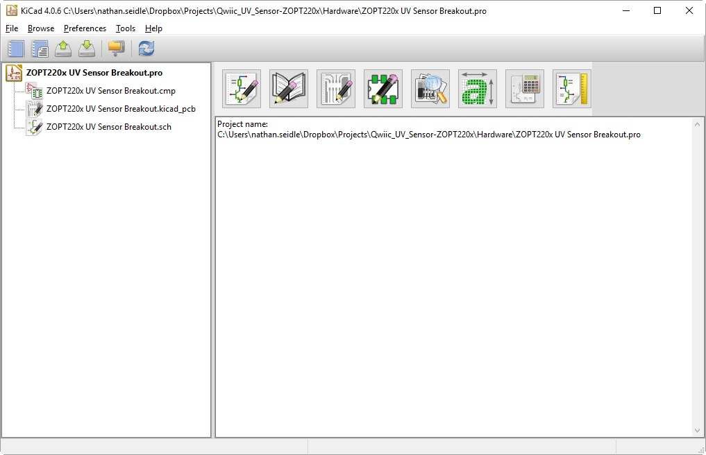
What are all these files?
These four files are all you need to share a KiCad design with a fellow collaborator. You may also need to share a footprint file, which will be explained more later on in this tutorial.
You may have had your first critical-judgment-eye-squint. Why is there a file to define which footprints go with which schematic components? This is fundamental to KiCad and is very different from how EAGLE works. It's not a bad thing, just different.
Double click on the schematic file with Kicad's Eeschema schematic editor. You'll probably get an error:
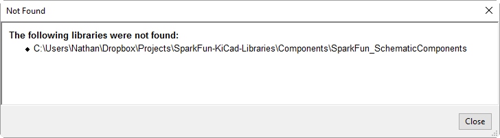
Ignore this for now. Click 'Close'.
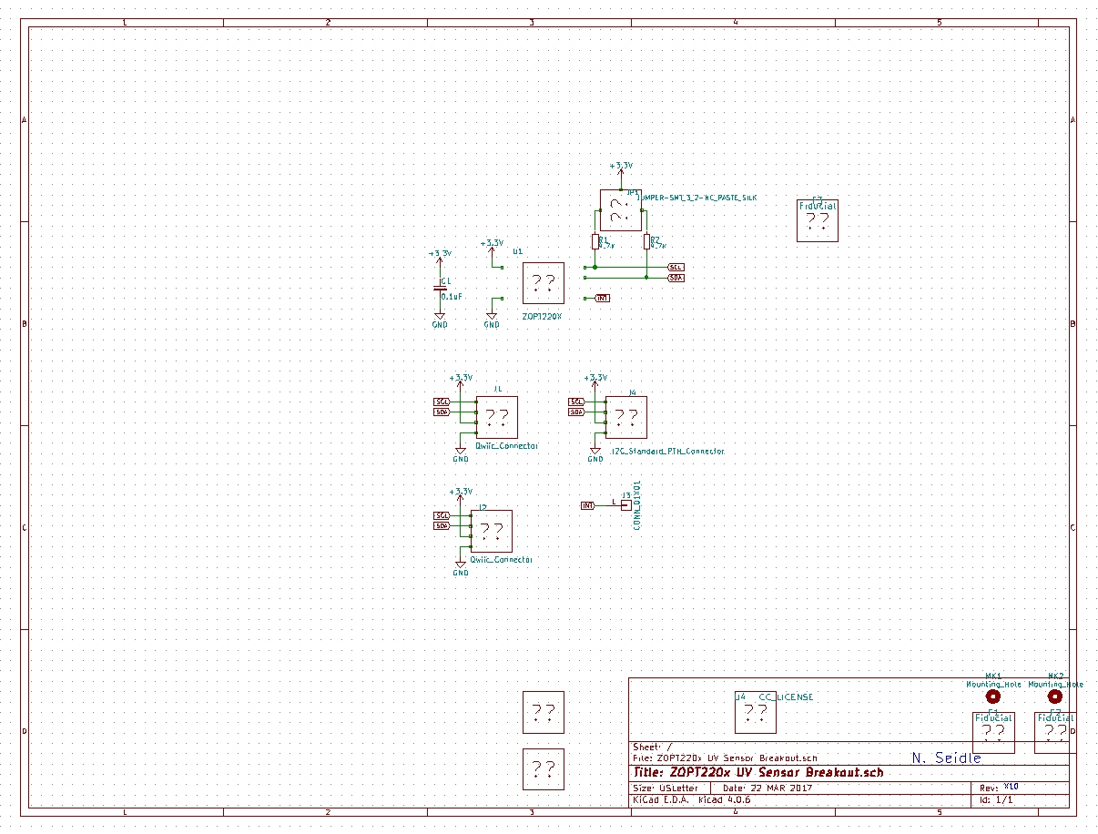
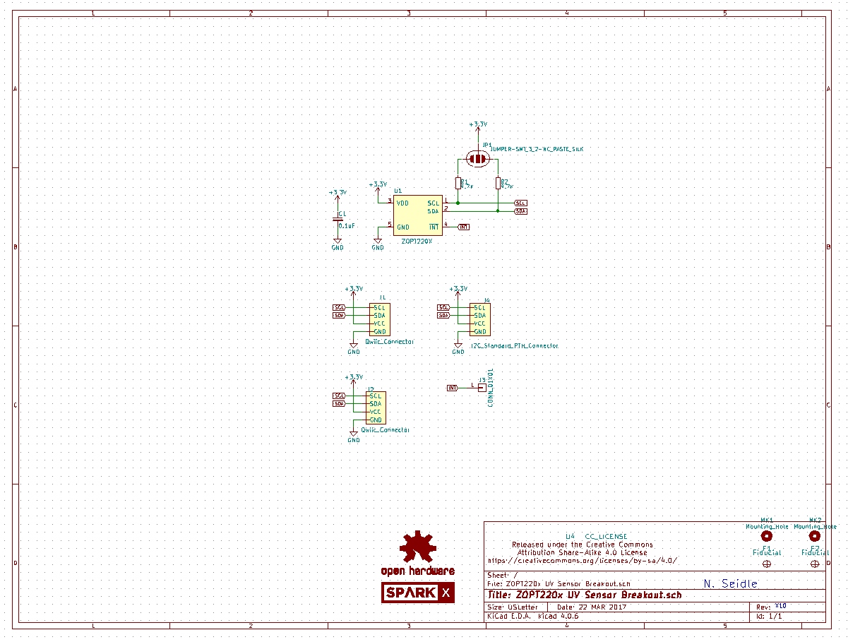
The schematic will load with lots of components with question marks (i.e.??). KiCad is missing the link to the devices within this schematic. Let's get them linked!
From within EeSchema, click on Preferences -> Component Libraries. This will open a new window. In the image below you can see that the project file contains information about where it should look for "Component library files". Each project has its own connections to different file structures. We need to tell this project where to find the symbols for this schematic.
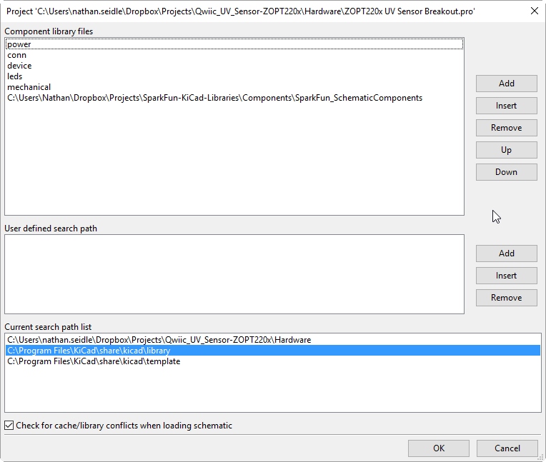
We will need the SparkFun_SchematicComponents.lib file. Download and store it in a local directory:
From the KiCad window, click the top 'Add' button. We'll show you how to create your own schematic symbols in a bit.
Navigate to the directory where you stored the SparkFun_SchematicComponents.lib file and click 'Open'. This file contains all the schematic components.
Once you've added the SparkFun schematic components library file, you should see it added to the list.

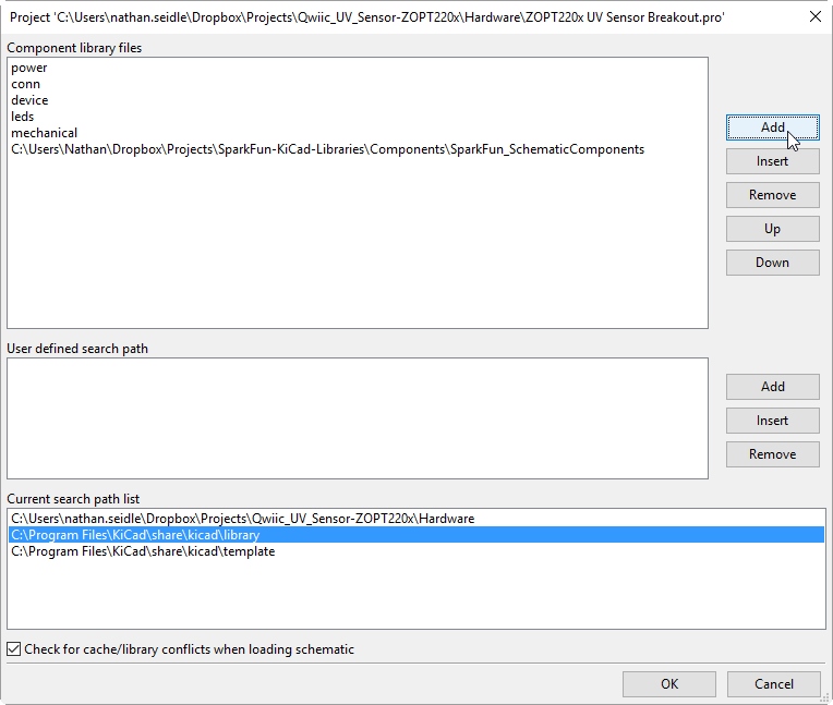
The astute will note the slightly different directory structure in the window:
C:\Users\Nathan...
and
C:\Users\nathan.seidle...
That's the difference between my home PC and my work PC. To avoid future errors when opening this schematic, let's remove the entry from the active library files. Highlight the C:\Users\Nathan... entry from the list and click on the 'Remove' button.
Click on 'OK' to close out the Component Libraries manager. Now close and re-open the schematic to refresh.
Congrats! No more ?? boxes. For more information about using schematic component libraries across multiple computers, check the next subsection about the "user defined search path." Otherwise, let's start editing the schematic!
The schematic component libraries are assigned using KiCad's Component Library Manager. If you're like me and have schematic libraries shared across multiple computers, adding a "User defined search path" is helpful:
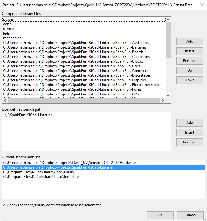
In the image , I have "..\..\SparkFun-KiCad-Libraries" defined. This is the local relative path to a Dropbox folder. These component library paths are specific to this project and *.pro file. When I open this project on my laptop, it will first look for the files in the "C:\Users\nathan.seidle..." location. It will fail and then search the relative path of "** ..\SparkFun-KiCad-Libraries**" and find the files. It allows me to share libs between computers and between GitHub repos without having to reassign the libraries every time I open the project on a different computer.
For now, you should continue with the tutorial. In the future, you may want to revisit this if you use KiCad across multiple computers.
If I get you to do nothing else, I will get you to learn the keyboard shortcuts! Yes, you can click on the equivalent buttons. However, the speed and efficiency of KiCad really shines when muscle memory kicks in so start memorizing. Here are the keyboard shortcuts in KiCad's Eeschema that we will be using frequently in this tutorial:
This breakout board needs a larger 4.7uF decoupling cap (because I say so). Let's add it!
Press 'a' to add a device to the schematic. This will open the component window. (If you are using a different tool you may need to click on the schematic as well):
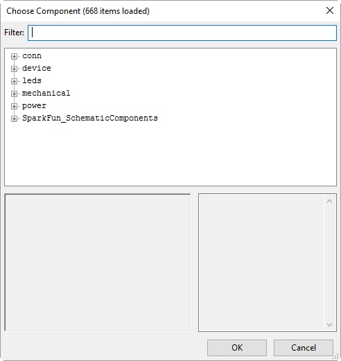
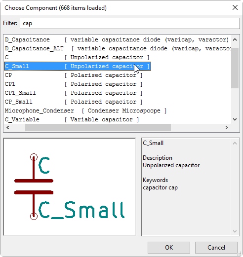
There are hundreds of components (668 items according to the title bar). Feel free to dig around but to quickly find what we need type 'cap' into the field Filter:. Select the device labeled as C_Small from the device library. Then hit enter or click 'OK'.
Place it on the schematic next to the 0.1uF cap.
After you place the capacitor, you'll notice you're still in placement mode. Hit the 'Esc' button on your keyboard to return to normal pointer mode. I find myself hitting escape twice a lot just to be sure I'm back in default state.
Once in default state put your mouse pointer on top of the 3.3V marker on the 0.1uF cap. Press 'c' to copy that device and place it above the new capacitor.
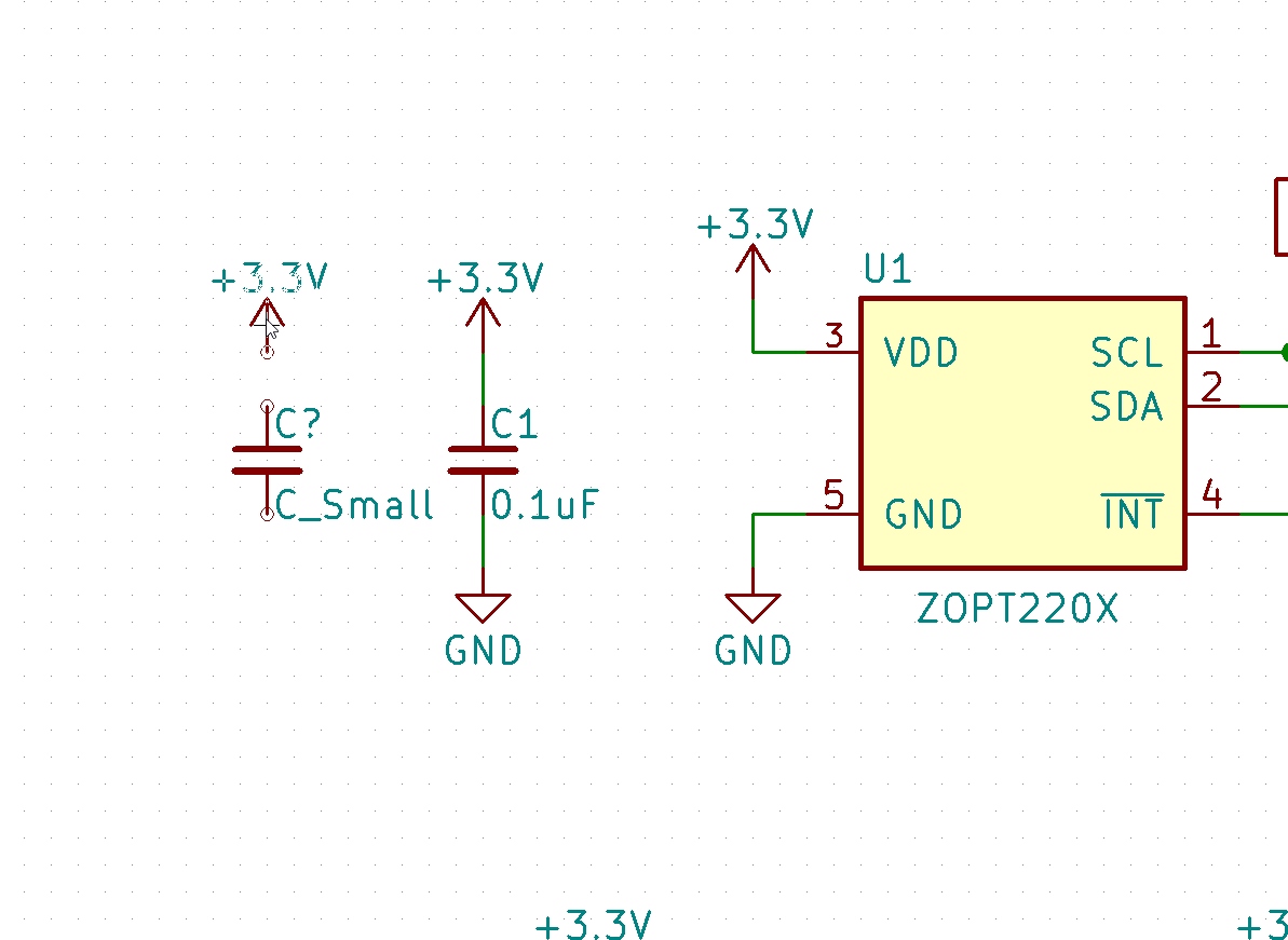
Do the same for the ground marker. Press 'ctrl+s' to save your work.
Now let's wire them together. You guessed it, press 'w' but here's the catch: have your mouse pointer over one of the bubbles before you press 'w'.

Move your mouse to the other bubble and left click on the mouse to complete the wiring for GND. Remember if you mess up, press 'Esc' once or twice to return to default. Then move your mouse pointer to the bubble you want to connect and press 'w' and begin wiring 3.3V. The shortcut 'w' stands for wire.
Did something go wrong? Use 'ctrl+z' liberally to undo any mistakes.
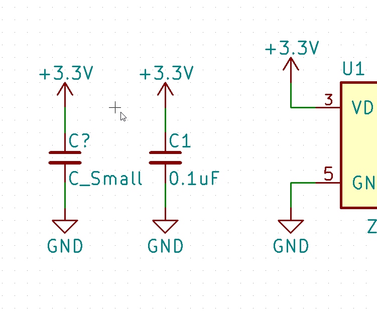
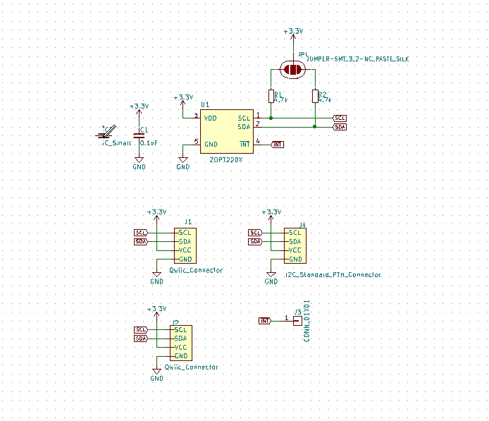
Power and ground are now connected to our capacitor.
Let's change the value from C_Small to 4.7uF. Hover the mouse pointer over C_Small and press 'v' (for value change). Change C_Small in the Text field by typing 4.7uF. Then hit enter or click 'OK'.

Congrats! You've just wired up your first schematic component. Press ctrl+s to save your work.
But what about the C? designator?! Don't worry about it! One of the many benefits of KiCad is the ability to auto-annotate a schematic.
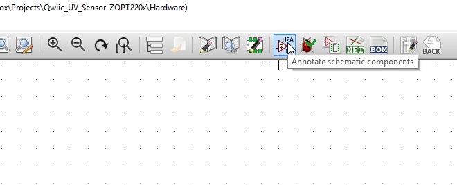
Click on the Annotate schematic components button.
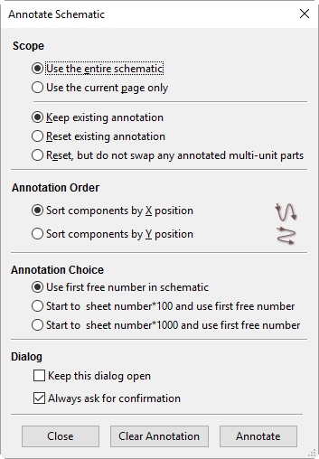
Use the default settings and simply click on Annotate button to confirm.
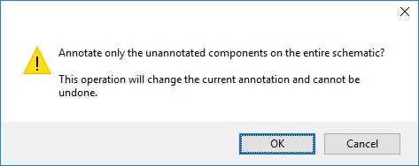
KiCad will ask you if you're sure, simply press return or click 'OK' again.

Capacitor with correct value and designator! We are all set. Time to edit the PCB.
Before we start editing the PCB, here are the keyboard shortcuts in KiCad's Pcbnew that we will be using frequently in this tutorial:
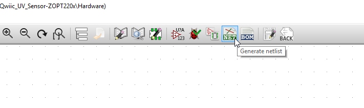
We've got our schematic, now let's get the new 4.7uF cap placed on the board. From the schematic, click on the 'Generate netlist' button.
You'll see the following window:
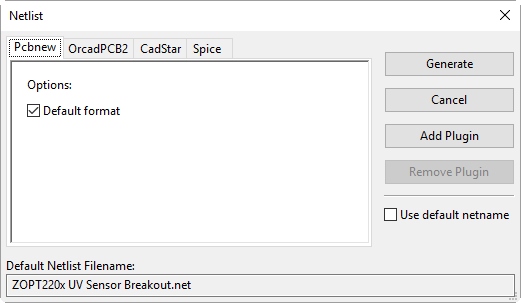
KiCad is powerful. And with this power, comes an overwhelming number of options. Lucky for us, we are just scratching the surface so we don't need to fiddle with any of these options. Simply press enter or click 'Generate' to confirm this screen. KiCad will ask you where you want to save the netlist as a ** *.net** file with the default location being the project folder. Again, press enter or click 'Save' to confirm.
Return to the main project window and double click the ** *.kicad_pcb** file.
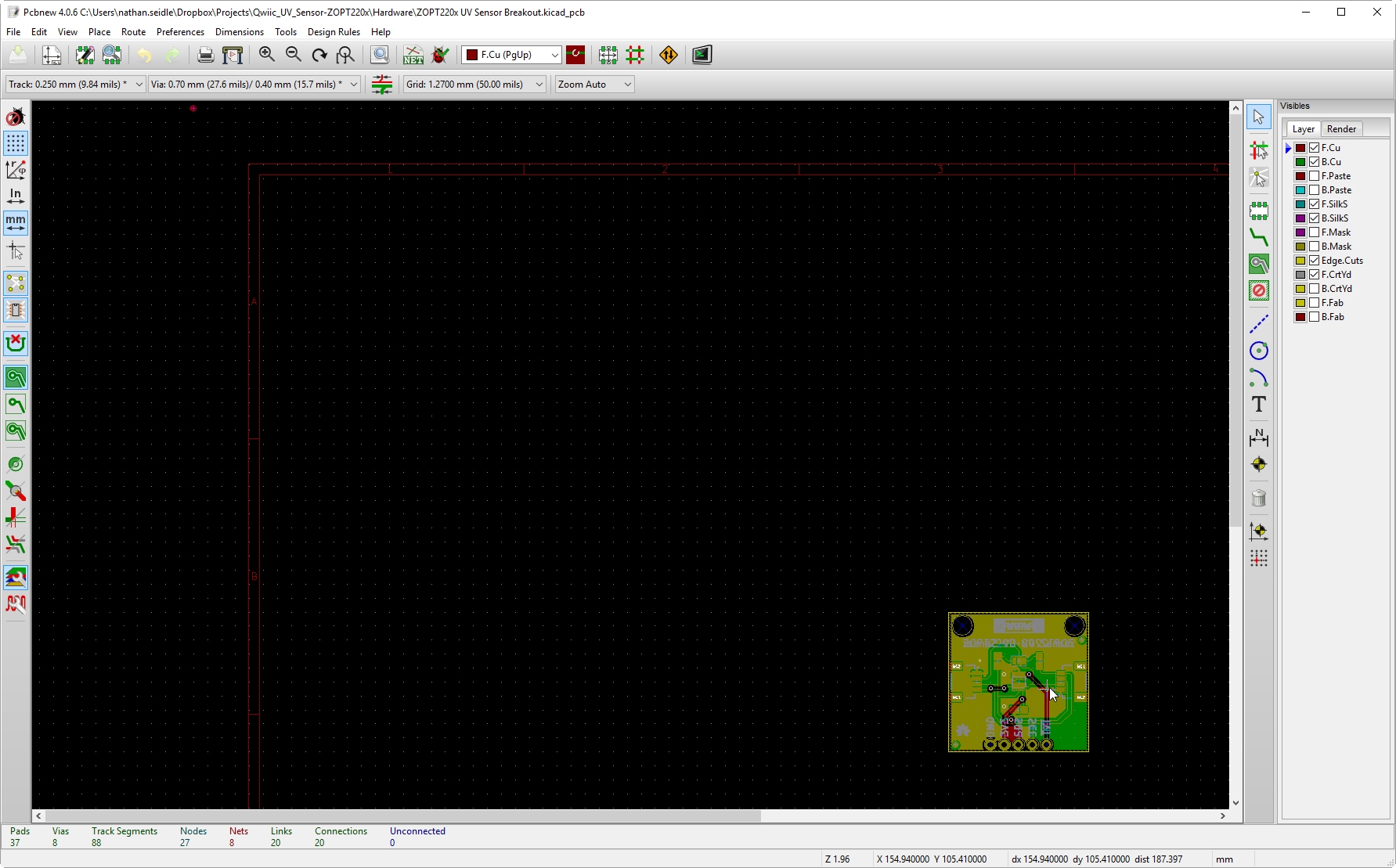
Welcome to PCB editing. Of all the differences between EAGLE and KiCad it was the look within PCB layout that threw me off the most. Under the View menu you will find three other views: Default, OpenGL, and Cairo. I prefer OpenGL. Lets switch Canvas to OpenGL for now.
Your mouse wheel does what you expect: Zoom In/Out and Pan by Clicking.
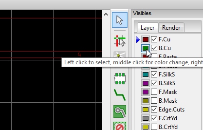
I don't like the layer colors! Ya, me either. To change the layer colors, on the right side menu use your mouse wheel to click on the green square next to B.Cu (bottom copper layer). I prefer the following layer colors:
Pressing '+' and '-' will switch between top and bottom copper layers. This is useful when you need to view a certain layer.
It's all cosmetic but these layer colors make it easier for me to see what's going on.
Be sure to poke around the Render tab (next to the Layer tab), namely the Values and References check boxes.
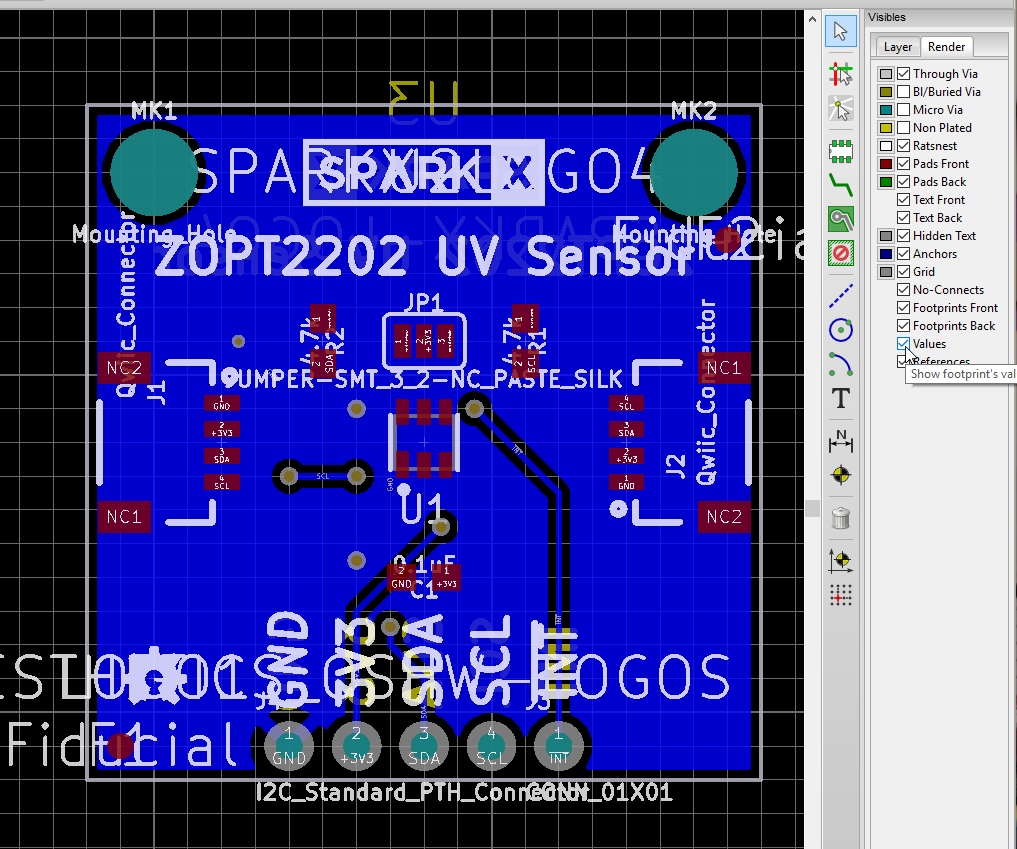
I find the Values and References extremely distracting when turned on so I leave them OFF. Many designers live and die by these values, so use as needed.
Aren't we here to add a 4.7uF cap to the board? Where is it? It's nowhere, sorry.
What's going on? We failed to assign a footprint to the capacitor we added in the schematic. Remember, KiCad does not link schematic components to footprints the same way EAGLE does. We have to specifically connect a footprint to each schematic component that was added.
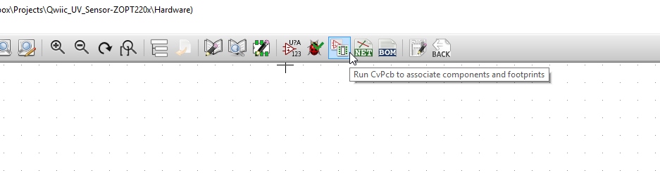
Navigate to back to schematic and click on the 'Run CvPcb' button to associate components and footprints:
If this is the first time you've run CvPcb you'll get this warning:
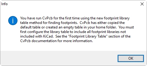
Simply click through it.
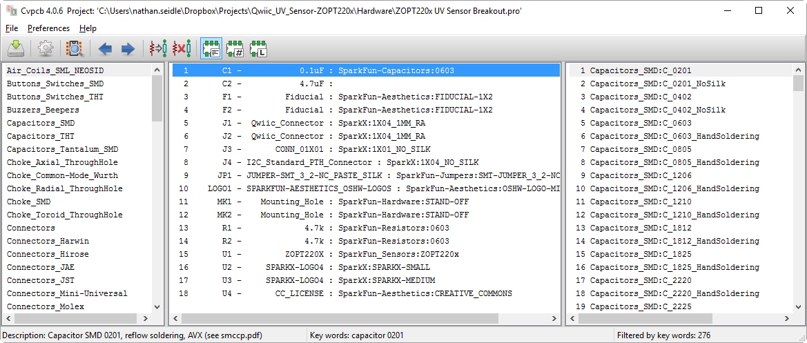
Depending on how many libraries you have installed, this may take up to 30 seconds. We will make this better later in the tutorial but for now, be patient.
In the left column is all the footprint libraries that KiCad ships with. In the middle is the list of components in your schematic. On the right is any footprint that may work with the highlighted component in the middle. Your job is to double click on the footprint on the right that goes with the component in the middle.
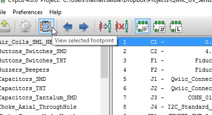
To make life easier click on the 'View selected footprint' button.
Now you can preview the footprint as you click down the list in the right.
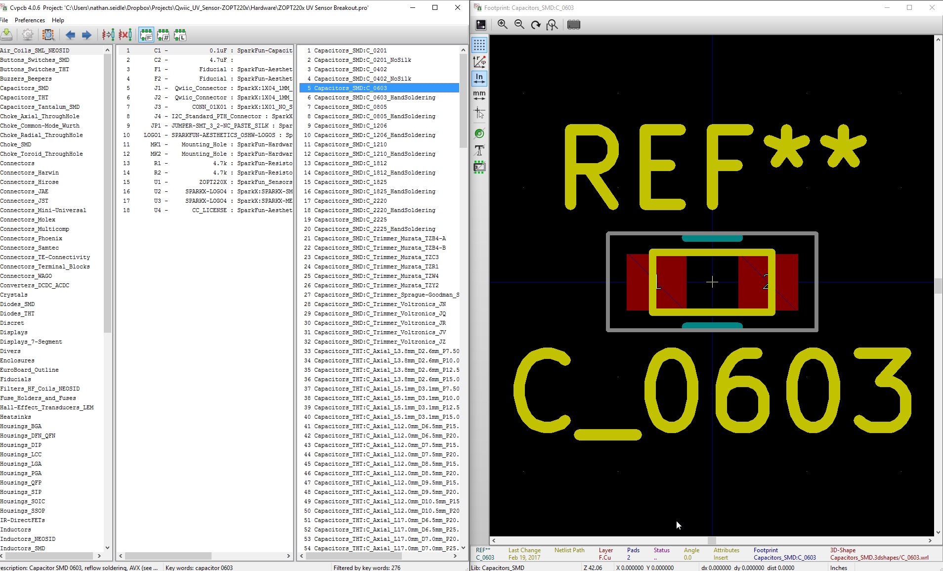
In Windows, I press and hold the Windows button and press the left arrow and release. This will lock the CvPcb window on one side. Then select and lock the Footprint Preview Window to the right. This allows us to flip through footprints in the left window while seeing the preview on the right.
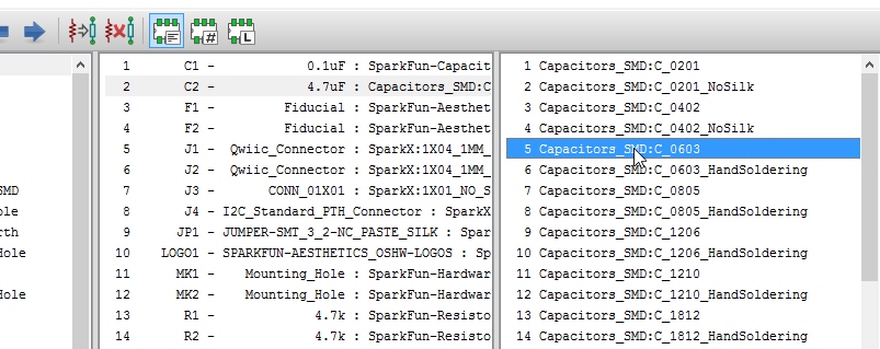
Highlight C2 in the middle column. Then double click the Capacitors_SMD:C_0603 in the right column. C2 should now be assigned a footprint.
Close the CvPcb window and click 'Save and Exit'. We need to re-export the Netlist. Remember how to do that? Click the 'Generate netlist' button again, press enter twice. Open to the PCB editor either from the schematic or from the project window.
Hey! It's still missing! We changed things, so we need to import the netlist! Remember how? Click on the 'Read netlist' button and you should see this window:
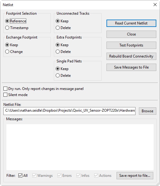
Click 'Read Current Netlist' and 'YES' to confirm. You can also hit enter twice. You should see the new capacitor near the board.
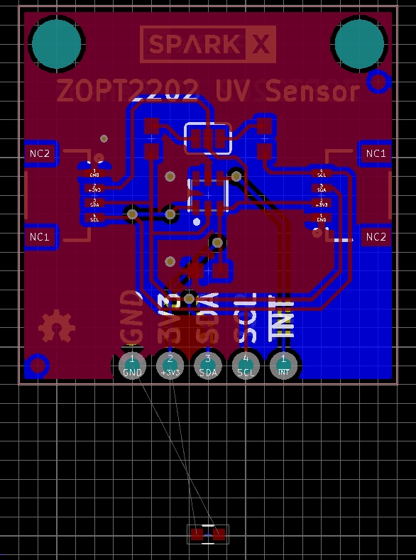
This is a decoupling cap so let's put it next to the 0.1uF cap that is already there. Start by hovering over the new cap and press 'm' for move.
Left click to place the capacitor. Now press 'm' over the 0.1uF cap in the way by moving it to the left.
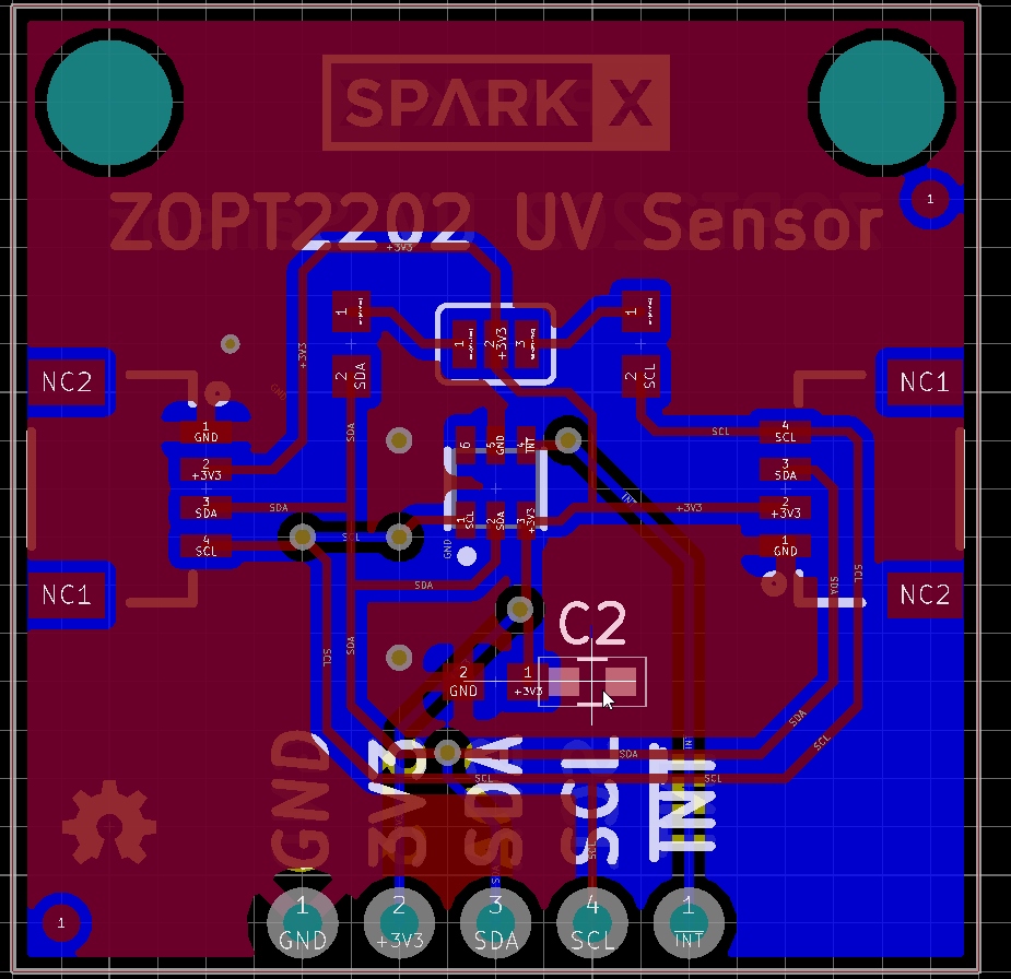
Press 'b' to update the GND polygon pours.

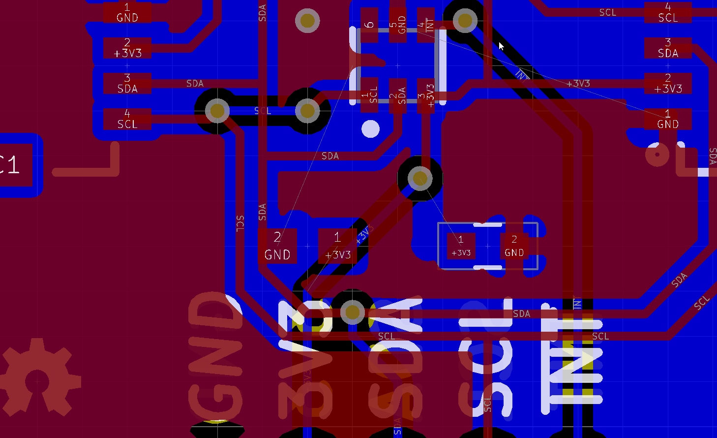
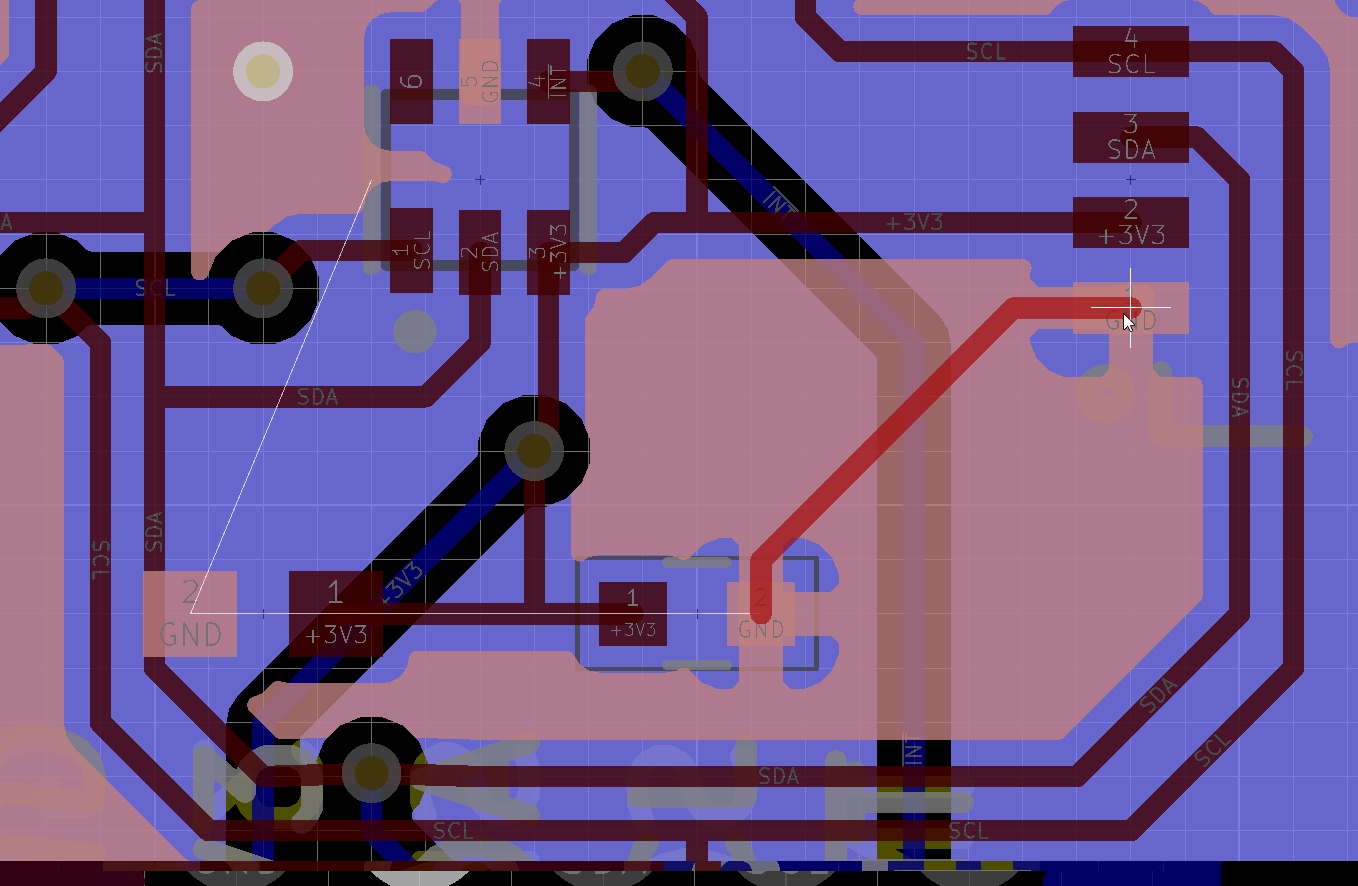
We've got some traces to fix but this isn't too bad. Hover over the bits of traces that you want to remove and press 'Delete'. Let's delete the trace and via that is under the capacitor's +3v3 terminal. If your pointer is over multiple items (as shown in the image below with the cursor over both the trace and capacitor), KiCad will pop up a menu to clarify your selection. This is basically asking you to pick which one you want to operate on.

If you ever run into a problem press 'Esc' to return to default pointer mode. If you ever delete something wrong press 'ctrl+z'.
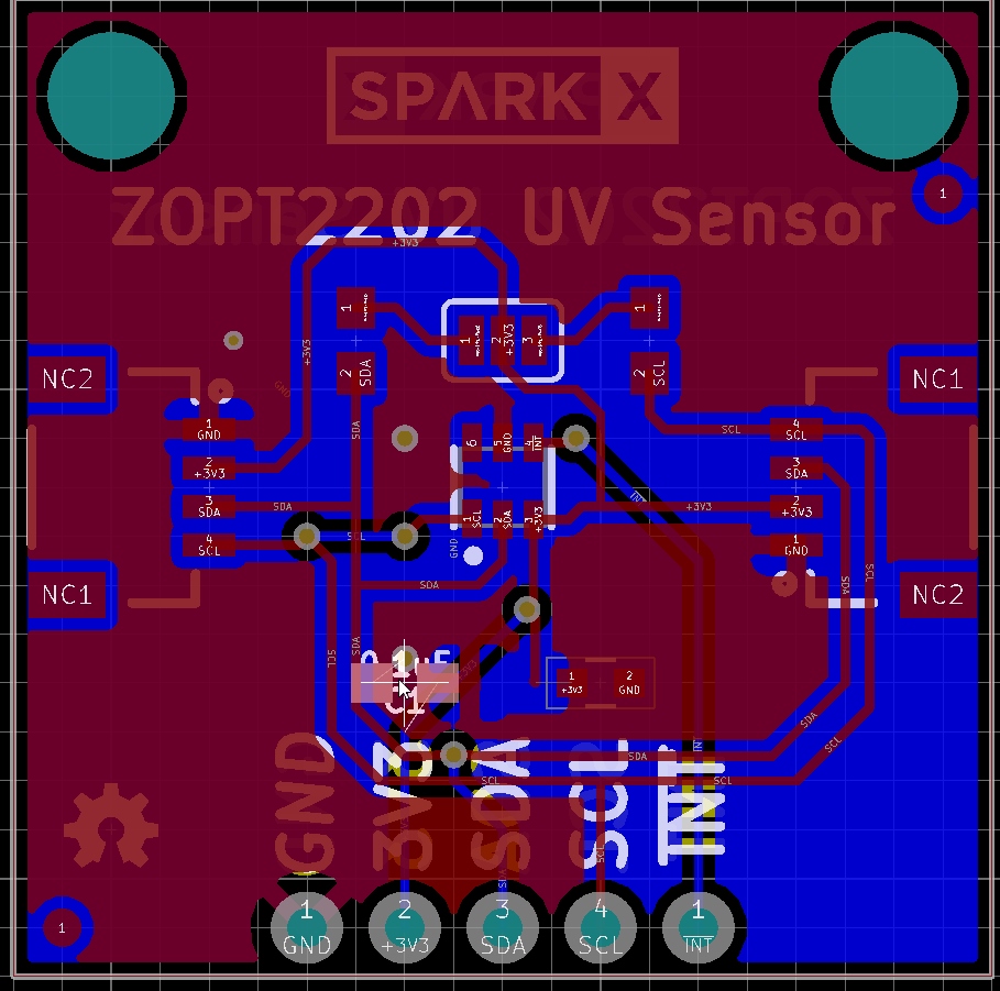
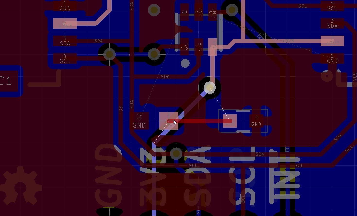
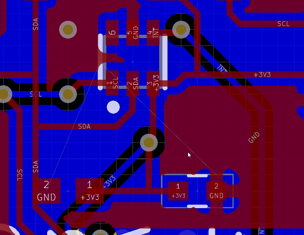
Once you've removed most of the offending traces, you can begin routing by pressing 'x'.
Single click on the pad that has the gray air-wire and drag it to the pad that it needs to connect to. Single click again to lock the wire in place. Press 'b' to update the polygons.
In the image below, KiCad is trying to route this trace in an odd way. If we place the trace here it will create an acute angle which is generally bad (read up on "acid traps"). We want the trace to be a T intersection. We need to change the grid.
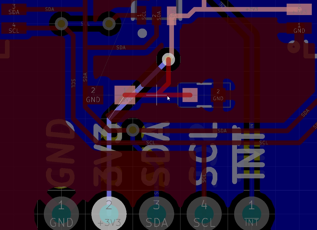
Press 'n' to go to the next grid size. I needed to hit 'n' only once to go to the 0.25mil grid to get this nice intersection, you may need to get to a finer grid. You can also find this in the menu options under "Grid: 0.0635mm (2.5mils)."
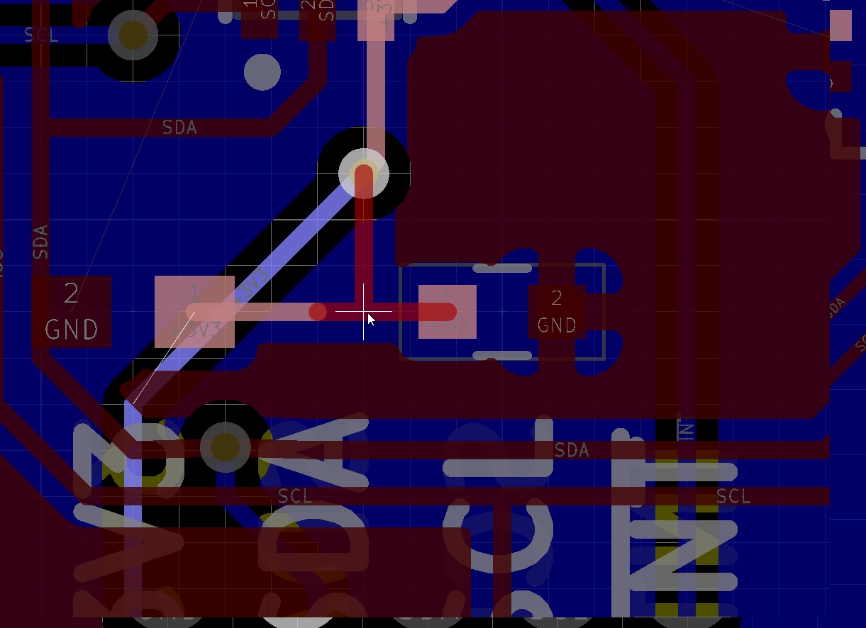
In the image below, I am routing the GND air wires. This is not really needed because the polygon pour connects the two pads but it does illustrate how good the 'magnetic' routing assistance is in KiCad. It's very quick and easy to go from pad to pad.
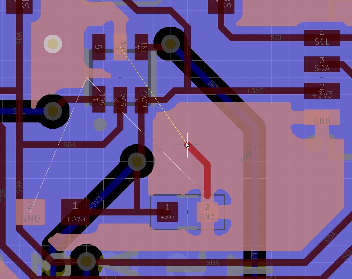
We have two air-wires left. To get these we'll need to place vias down to the bottom layer. Start by pressing 'x' and clicking on the start of the capacitor's air wire for GND again.
Bring the trace out.
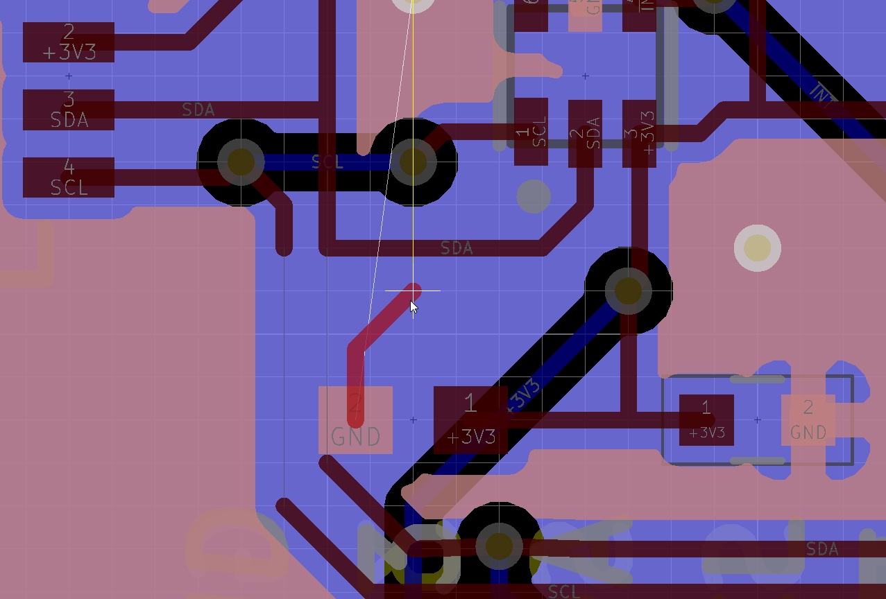
When you've reached open ground press 'v' to create a via. Single click to place the via and KiCad will automatically start routing on the bottom layer. Press 'Esc' to stop laying down traces; the polygon pour will take it from here. Pressing 'Page Up' will take you back to the top layer.

To get this last air wire, you can try clicking on the GND pad of the 0.1uF cap but annoyingly KiCad won't start routing?! Why?! It's actually a good thing: the SDA trace is too close (overlapping actually) to the GND pad on the 0.1uF cap. By not letting you start routing KiCad is saying that trying to put a trace here would violate the DRC rules. What to do? Rip up the SCL and SDA lines to make some room.
Aha! Much better. Press 'x', click on the capacitor's GND terminal, bring the trace out, and press 'v' to drop a via in this area. Hit escape to stop routing (let the polygon take care of it). Finally, press 'Page Up' to return to the top layer view.
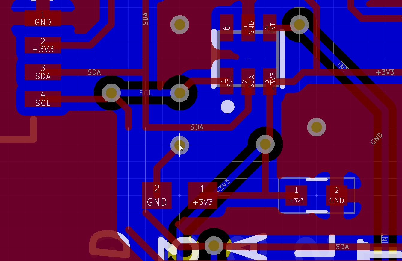
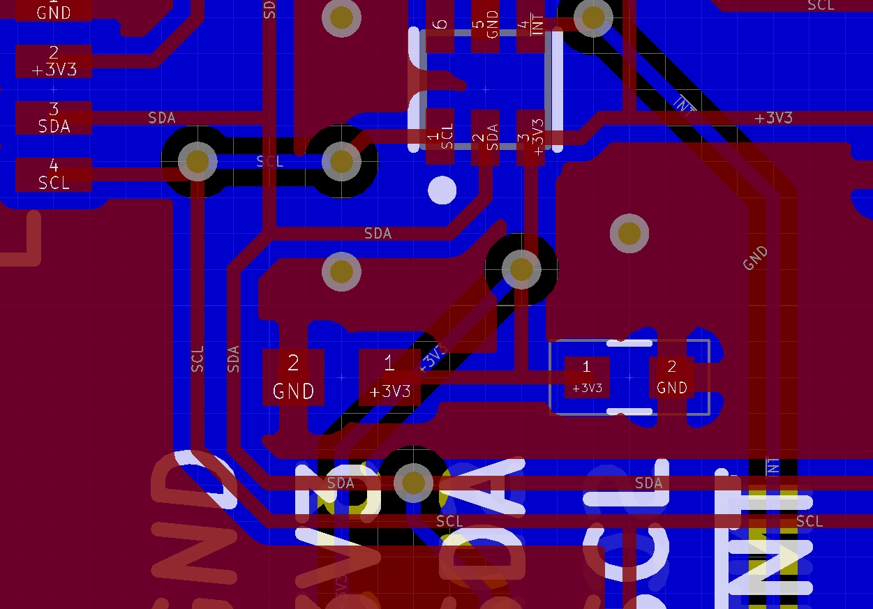
Use the 'Delete' and 'x' buttons to re-route the SDA and SCL lines to finish up this board. Then press 'b' to update the polygons. The board should look similar to the image below.
Congrats! We have finished routing the footprints. Now let's run the DRC to see if we're legal.
Before we continue let's go over the process for modifying or removing a component from a PCB layout. For example, let's say that you wanted to remove an extra capacitor or resistor from a design. You would do all the regular steps:
The difference is a few import settings:
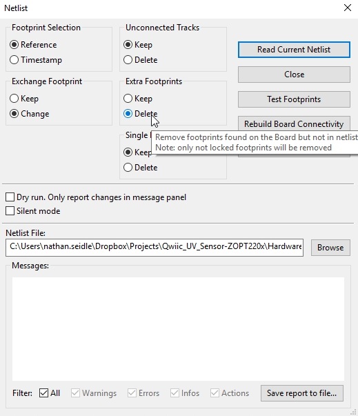
During the netlist import the default settings are to 'Keep' exchange footprint and to 'Keep' extra footprints.
Here, we need to change two things:
You may also want to 'Delete' unconnected tracks to clean up any left over tracks from the component you removed.
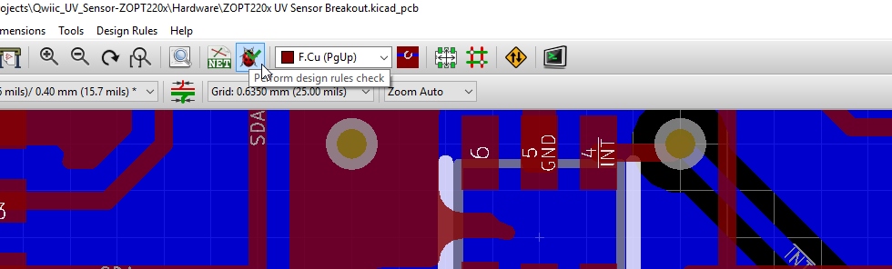
Click on the ladybug with the green check mark on it to open the Design Rule Check (DRC) window.
Let's take a moment to talk trace width, trace spacing, and vias. In general, SparkFun designs boards with:
We go smaller than this on many designs but if you're designing your first PCB, do not design it with 4mil traces and 8mil vias. You shouldn't need to go that small on your first board.
Making PCBs is tricky and for each increment of tolerance you remove you increase the chances that the PCB (proto or not) will be fabricated with an error. And those errors can be hard to identify. We design with 10mil trace/space in order to insure and reduce the probability that we'll see PCBs with errors on the production floor. There's nothing worse than troubleshooting a faulty product and asking yourself: "I've tried every rework and soldering trick in the book, is it the PCB that's bad?"
That stated, we are seeing many PCB fab houses charge low prices for 7mil trace/space and 12mil vias. If you've got a complex board with tight layout challenges, it's better use the smaller trace/space and vias. Save yourself the layout time and rely on the PCB fab house to correctly fabricate your board.
We generally use the KiCad defaults of:
Press enter again to run the DRC with the default settings.
Aw shucks! What's wrong with my board? The vias marked with red arrows are too close to the traces near by. The error message will show up in the window as an error indicating: "Via near track." Fix them by ripping up (press 'Delete') any traces near the vias and re-route them (press 'x').
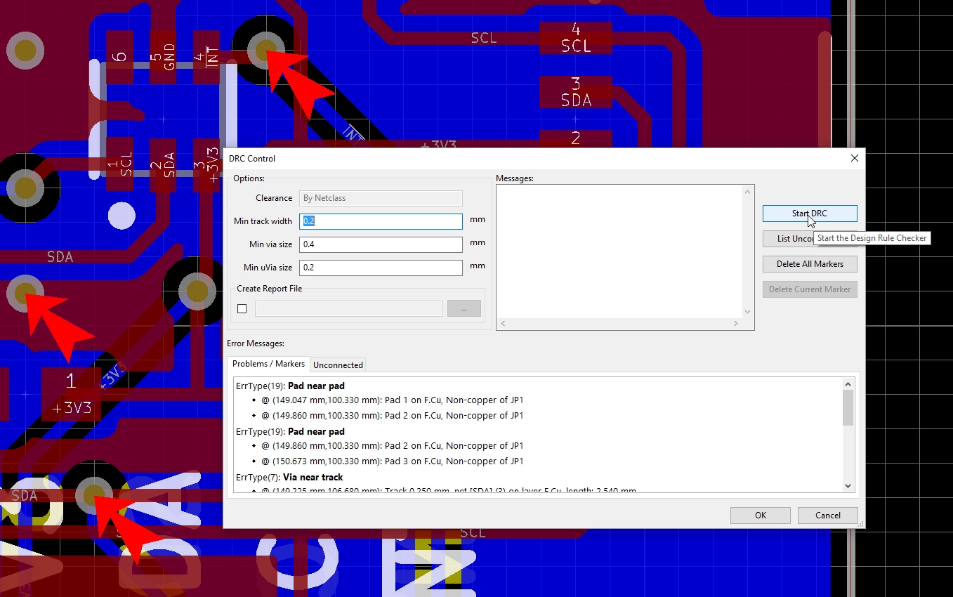
After adjusting the traces causing the issues, re-run the DRC. These three flags should disappear.
Congrats! You've fixed those "Via near track" issues.
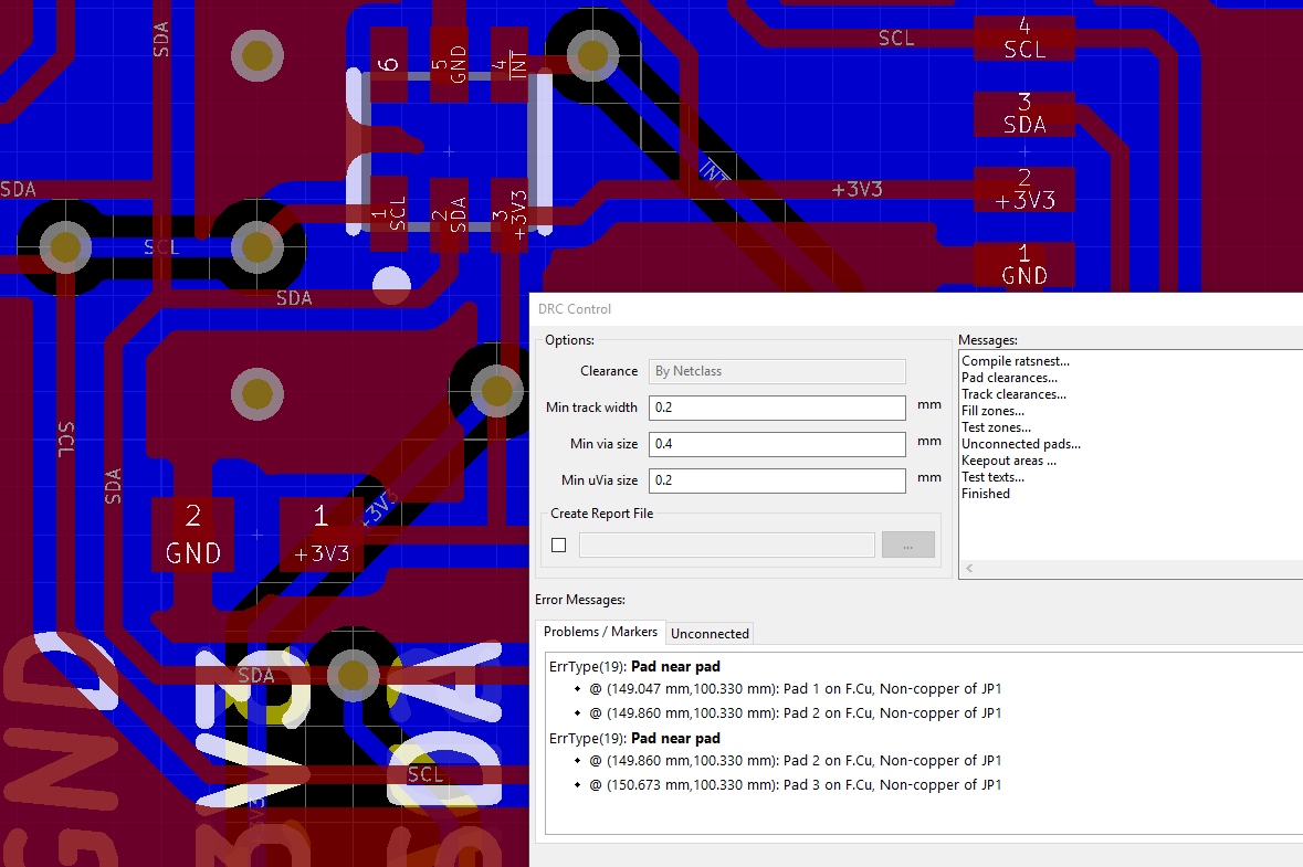
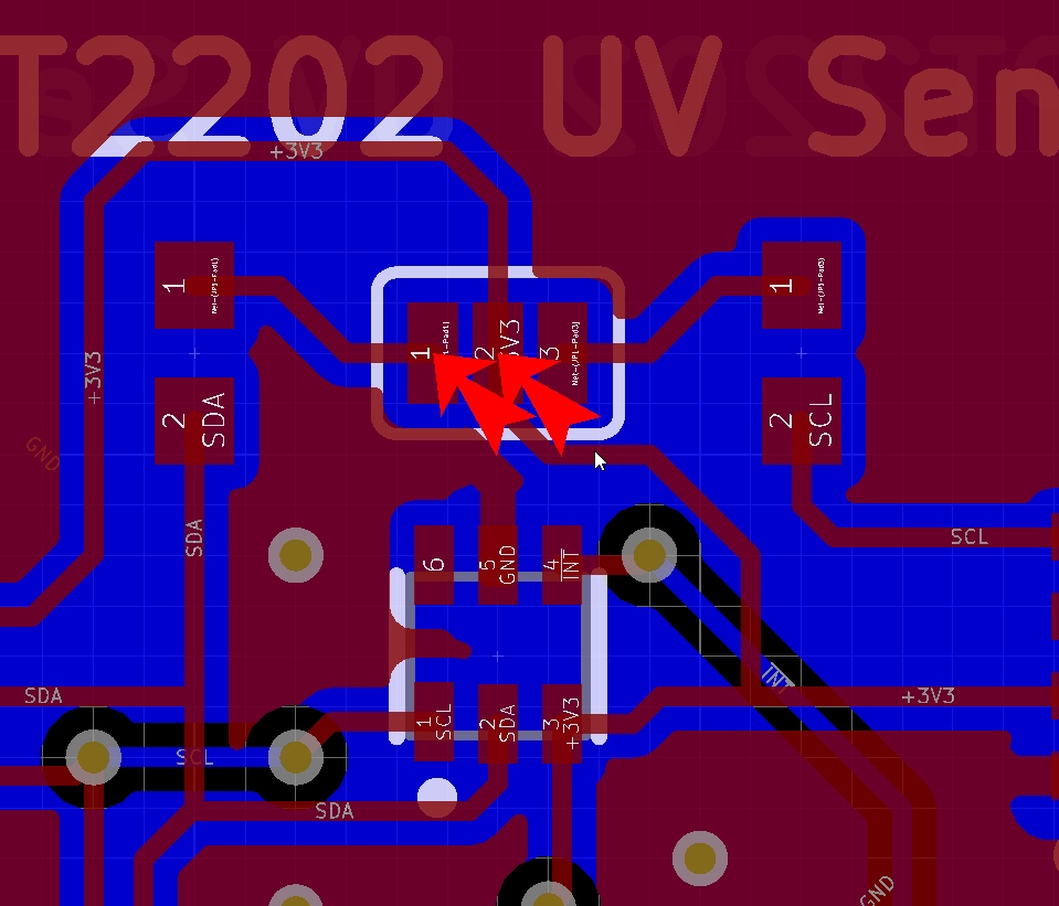
But wait, we are not done yet! There are still two DRC error arrows left with the error indicating: "Pad near pad". KiCad is trying to tell us the pads on this solder jumper are too close together. SparkFun has used this footprint for years and is comfortable with the design so let's change the Netclass clearance constraint.
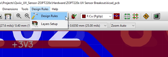
Open the DRC rules from the Design Rules menu.
Here is where you can create specific rules for specific traces and classes of traces. The problem that we are running into is the Default Clearance is 7.9mil (0.2mm). If we decrease this to 7mil (0.1778mm), click 'OK', and re-run the DRC...
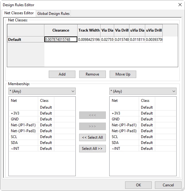
DRC errors resolved! Now reducing the DRC clearances in order to get your board to pass DRC is not an ideal solution. We want the pads on the solder jumper to be close enough to be easily jumpered with solder so increasing the distance between the pads on the footprint would be counterproductive. In general, you should set your DRC rules and stick to them.

One last note about DRC: Leaving airwires on your PCB is a sure fire way to generate coasters (bad, unusable PCBs).

From the DRC window there is a 'List Unconnected' button. This will show you the location of any unconnected traces (I had to rip up the SDA trace on the bottom right side of the PCB to show this error). It's very important that you check for airwires before ordering your PCBs. As you progress through your layout, I recommend focusing on the 'Unconnected' count at the bottom of the screen (circled in pink). If you think you are done routing a board but still show a few unconnected wires that you can't find, the DRC window will help you locate them.
Press 'ctrl+s' to save your work.
Well done. You've made it through design rule checking! Now it's time to order boards.
We added a component to the schematic, we modified the PCB layout, and we checked for errors. Now we are confident and ready to have our boards made! Time to export the gerber files.
Gerber files are the 'artwork' or the layers that the PCB fabrication house will use to construct the board. We've got a great tutorial on the different layers of a PCB so be sure to read up if all this is new to you.
Click on the 'Plot' button next to the printer icon in the top bar to open the 'Plot' window.
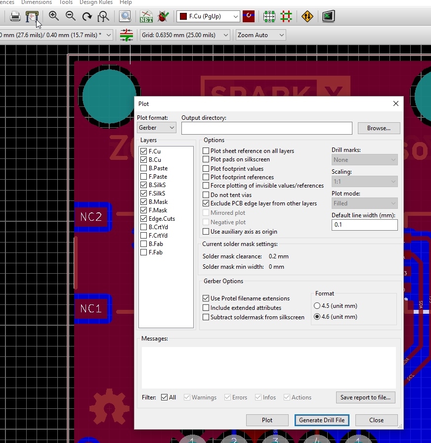
In general, there are 8x layers you need to have a PCB fabricated:
In the Plot window with the Plot format set for Gerber, be sure these Layers are checked:
Additionally, click on 'Generate Drill File' button. You can use the defaults here as well. More on the PTH vs. NPTH check box in a minute. For now just click 'Drill File' or press enter to generate the drill file.

Click on 'Close' in the 'Drill Files Generation' window.
Click 'Plot' to generate the gerber files for the layers and then click 'Close'.
This is the last chance to catch any errors before paying real money. Reviewing the gerber layers often shows you potential errors or problems before you send them off to fab.
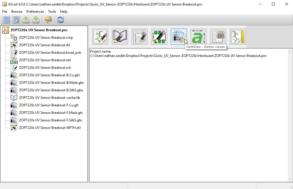
Return to the main KiCad project window and open up GerbView by clicking on the button.
Once KiCad's GerbView is open, click on File -> Load Gerber File. Select all the files shown and click Open.

Next, click File -> Load EXCELLON Drill File. Load your drill files by selecting the all the drill files shown and click 'Open'. They should be in the same directory.
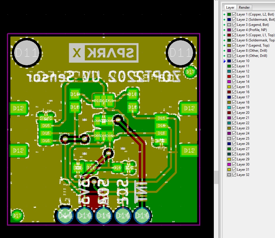
The layout looks very different but this is a good thing. You've been staring at your design for hours and it's hard for your brain to see issues. I generally do not change the layer colors unless I have to. I want the gerber review to be jarring and different from my layout practices so that I'm more likely to catch issues.
From this view, turn off all the layers but the Top Copper (layer 5). Additionally from the Render menu, turn off the Grid and DCodes. This will make the review less cluttered.
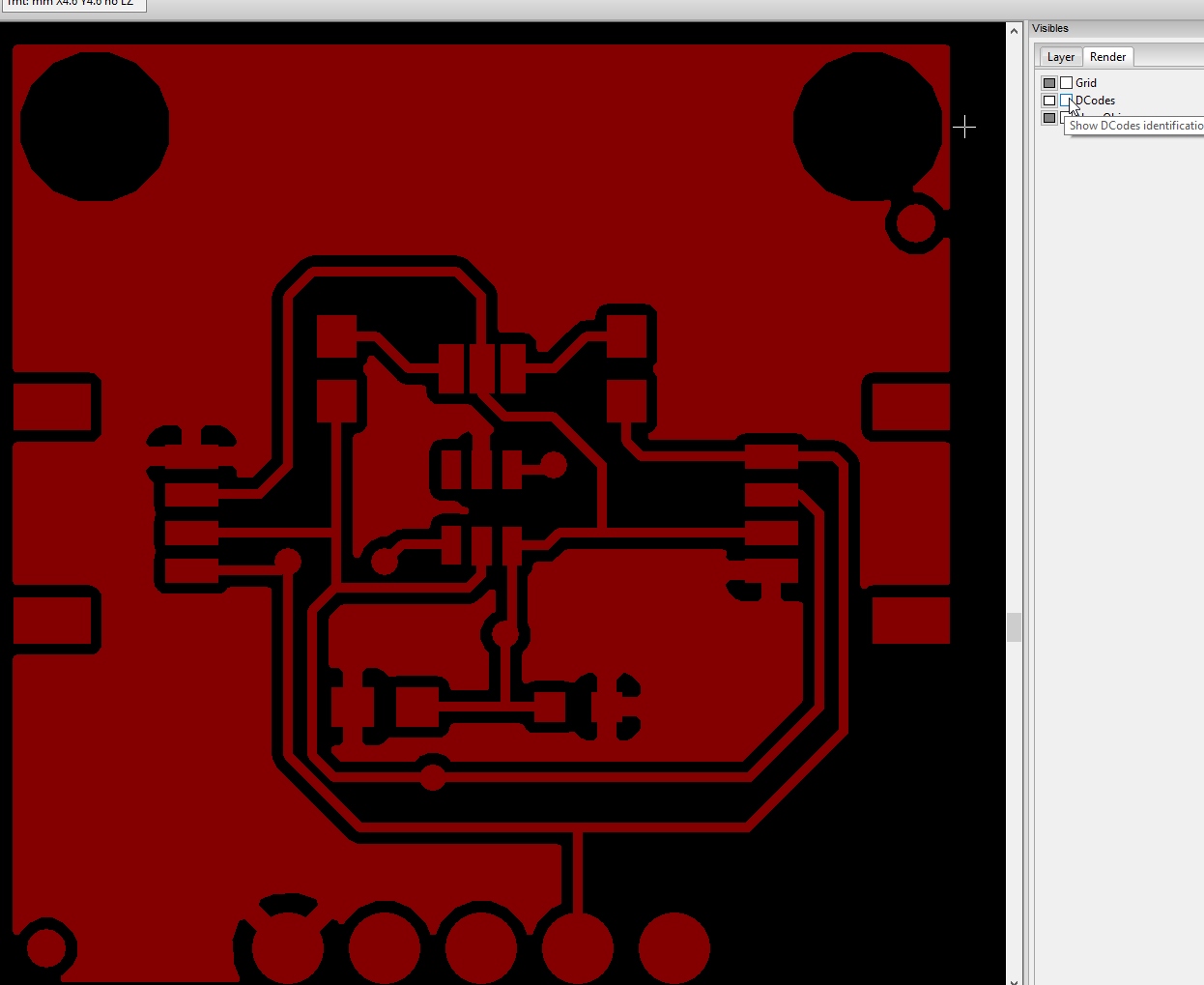
Now step through the different layers by toggling them on and off. You're looking for irregularities and things that look out of place. Here are some things I look for:

Now turn everything off and repeat for the bottom layers.
Did you catch it? There are a handful of things wrong with this example.
Leaving a silkscreen indicator off won't break your board but it's small defects like this that the gerber review is meant to catch.
Homework:
Take a moment and return to the PCB layout window to edit the make these corrections.
Now, we need to deal with the two drill files.
When generating the drill file for this design two files where generated:
Non-plated through holes are holes on your PCB that do not have copper covering the vertical walls of the hole. This is sometimes required for advanced designs where thorough electrical isolation is needed. However, it is rare. While plated through holes (PTH) are common and cheap, NPTH requires an extra step in the PCB fabrication process and will often cost extra.
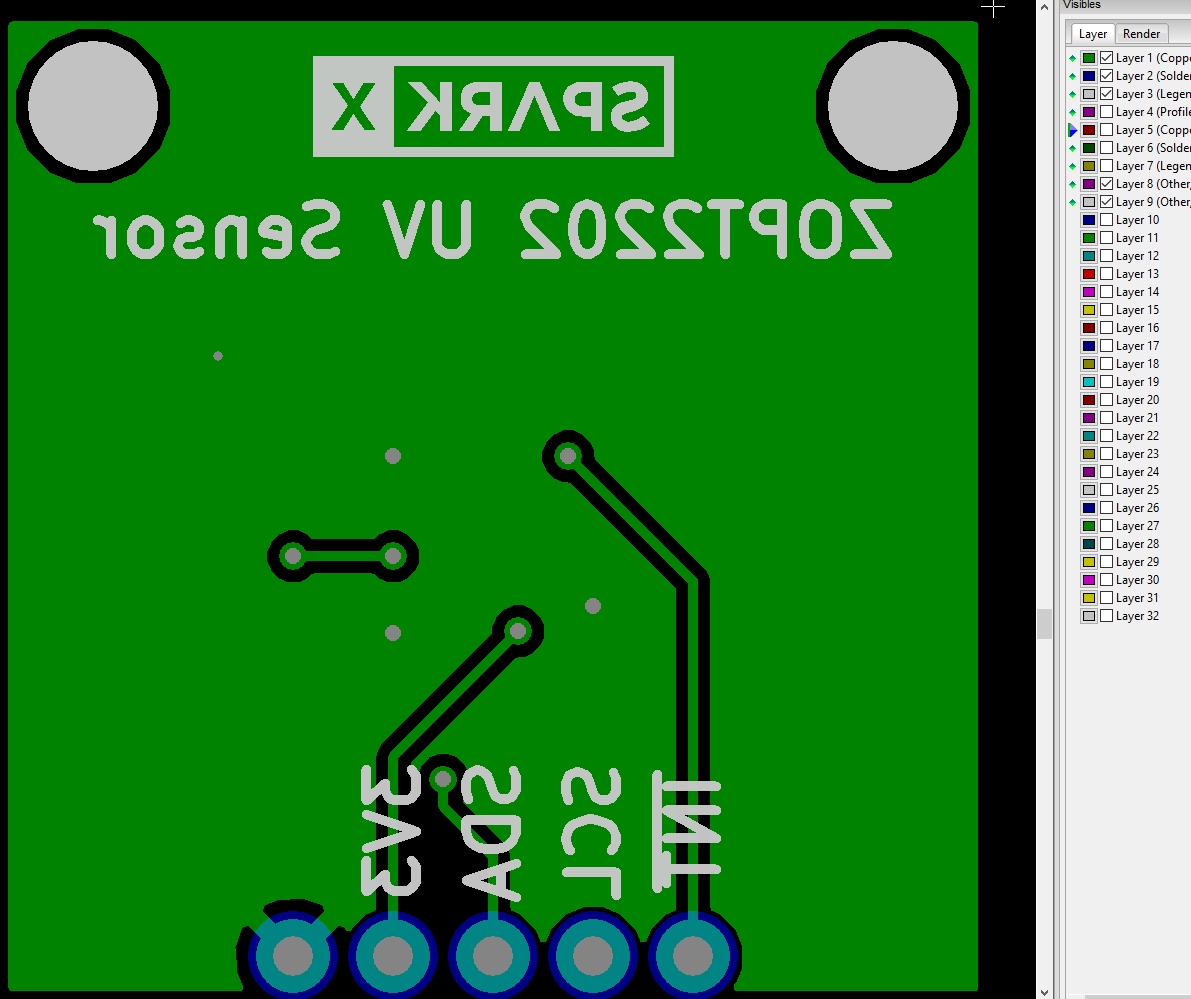
We don't need NPTH for this design, so what happened? The 'STAND-OFF' footprint (i.e. used for the drill holes top of the board for mounting holes) was imported from the SparkFun Eagle library and KiCad seems to think it is a non-plated hole for some reason.
To correct this go back to the PCB layout, click on the Plotter, click 'Generate Drill File' and select the box that says 'Merge PTH and NPTH holes into one file'. In a later section, we'll go over how to edit the 'STAND-OFF' footprint to use a regular PTH hole.
Are you doing SMD reflow? Need to order a stencil to apply the solder paste to your board? Turn on F.Paste in the Plot window to generate the top paste layer.
This *.gtp file is sent to a stencil fabricator to create the stainless steel or mylar solder paste stencil. If you're unfamiliar with stenciling solder paste we have a fabulous tutorial.
We use OSHStencils for our proto stencils. The top paste layer is not needed to fabricate a PCB.
If you're happy with your layout, let's order some PCBs! Every fab house understand and works with gerber files, so navigate to the directory on your computer where your KiCad project resides.
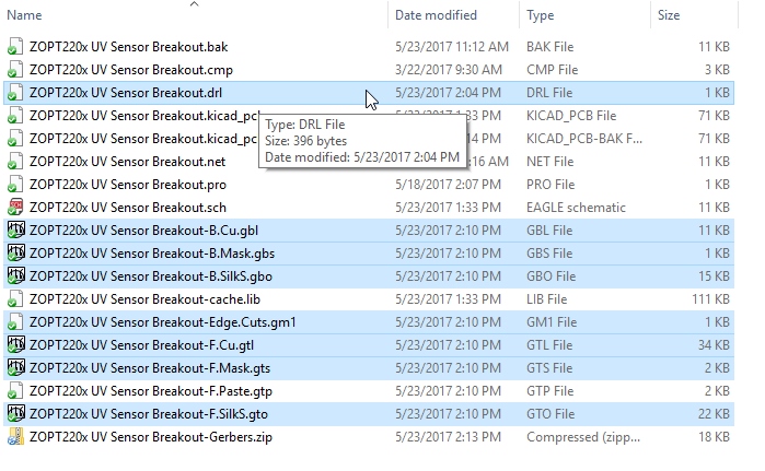
Select and zip the following 8x files:
You could zip all the files in the directory and send them off to your fab house but I don't recommend it. There are a tremendous number of PCB layout software packages generating all sorts of different file names and formats. It's often difficult to tell if ** *.cmp ** is a gerber file or something else. Does the customer care about the ***.gtp** file or is that just extra? It's better to give the fab house only what you want fabricated.
The final step? Order your boards! The gerbers are the universal way to communicate with a PCB vendor. There are hundreds if not thousands of PCB vendors out there. Shop around!
In addition to your gerbers, you'll need to specify via email or the PCB vendor's website various elements of the PCB:
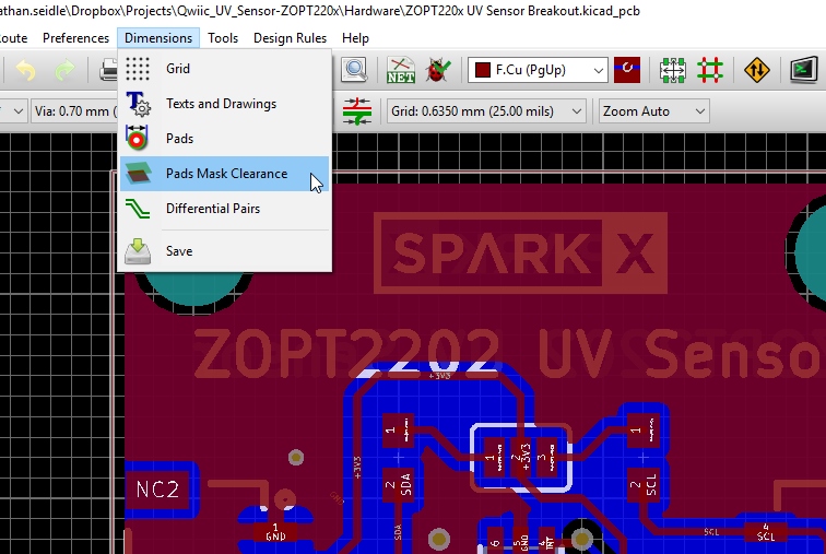
If you had a look at the soldermask on this PCB and wondered why it looked odd, you're not alone. Let's compare the PCB's soldermask for KiCad (as shown in green) and Eagle (as shown in pink). You should notice two things:

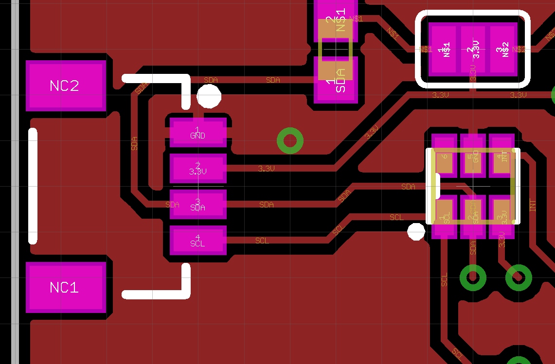
In the image below, we can see the SMD Qwiic connector within Eagle. The default soldermask clearance is 0.1mm per side in Eagle.

In KiCad's Pcbnew, open the ZOPT220x Breakout and click on Dimensions -> Pads Mask Clearance. KiCad's solder mask clearance has a default of 0.2mm per side. We recommend you change this value to 0.1mm. Most fab houses will use 0.1mm as their default as well. You will then need to re-export your gerbers and load them back into GerbView.
Making the clearance smaller than 0.1mm will cause difficulties for the fab house to get the registration correct.
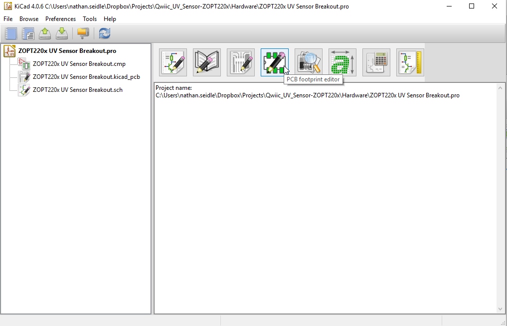
This section will show you how to create your own local custom footprints so that you can use them and connect them to schematic components using CvPcb. We're going to assume you've already been through the previous sections of this tutorial; you should have KiCad downloaded and installed.
Open KiCad's project manager and then click on the PCB footprint editor button.
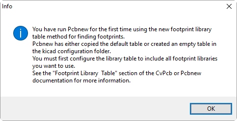
You may get the warning. That's ok, just click through it. This is KiCad's way of telling you it's going to create the default table of libraries that link to KiCad's extensive GitHub repos.
Click Preferences -> Footprint Libraries Manager. This will open the list of all the footprint libraries now accessible to you.
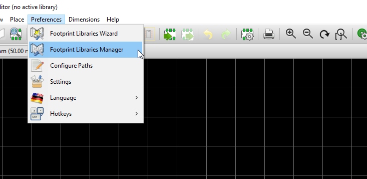
This is a tremendous list of libraries! Click 'OK' to close the manager.

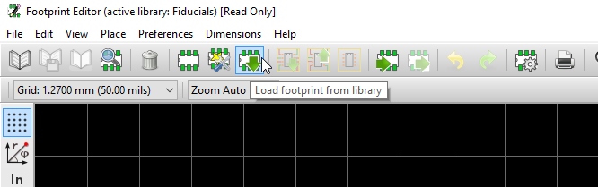
Let's poke around these libraries. Click on 'Load footprint from library' button and then 'Select by Browser'. This is a handy tool for perusing the available footprints.
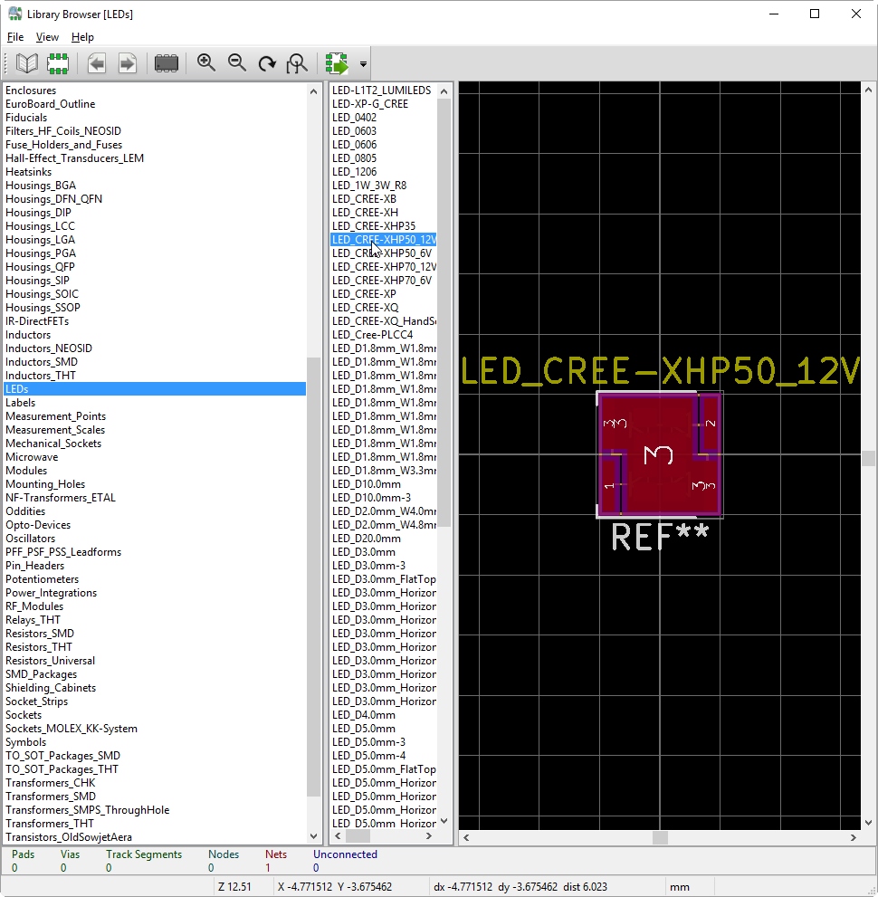
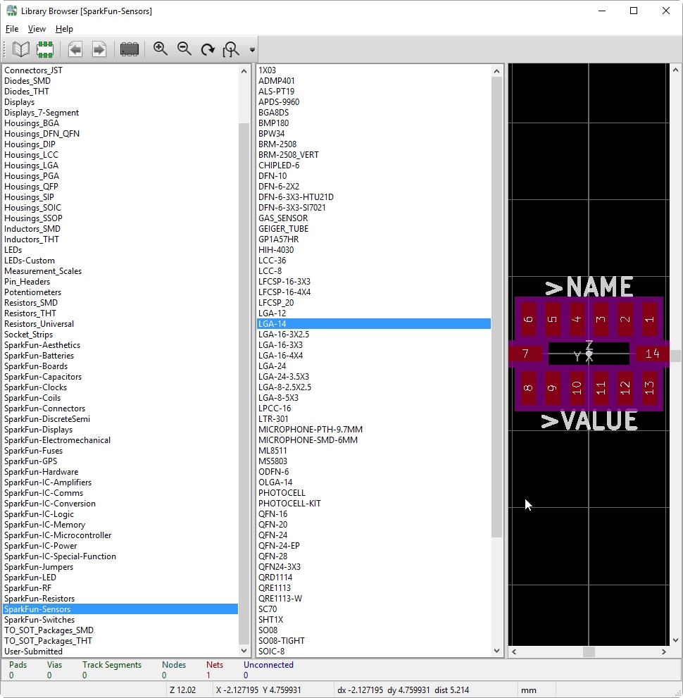
Navigate to the LEDs -> LED_CREE-XHP50_12V footprint. Here is an example footprint in LEDs library. Double click on this footprint to open it up in the editor.
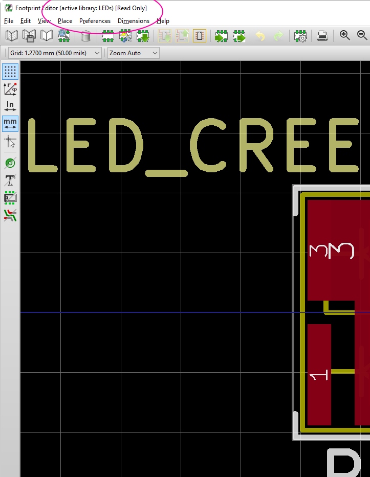
Note the title bar of the editor window has changed. The active library is now LEDs and it is read only. Obviously KiCad wants to control their libraries; not just anyone can save to their repos. If we want to edit this footprint we need our own local copy.
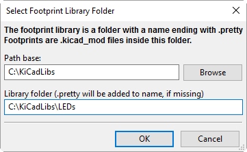
Let's create a local directory to keep all our local footprints. For this tutorial, please create a local folder called 'C:\KiCadLibs\' (or your platform's equivalent).
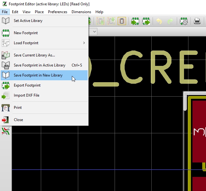
Now click on File->Save Footprint in New Library.
I recommend using different directory names for different sets of footprints (resistors, connectors, LEDs, etc). Select the 'KiCadLibs' folder that was created and then type '\LEDs'. KiCad will create the new 'LEDs.pretty' directory with a file 'C:\KiCadLibs\LEDs.pretty\LED_CREE-XHP50_12V.kicad_mod'. And we're off to the races. Except, not quite yet.
Notice the title bar in the Footprint Editor still states the active library is LEDs and is read only. We need to switch the active directory to our local folder. I'm going to head you off: File->Set Active Directory doesn't work as it only gives you the list of libraries that KiCad ships with. Oh KiCad!
Before we can set our new footprint directory as active, we need to make KiCad aware of it. Re-open the Preferences -> Footprint Libraries Manager.
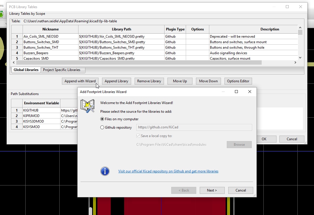
Click on the 'Append with Wizard' button. You'll be asked to locate the directory you want to add. In this case, we want to add the 'Files on my computer'. Click on the 'Next >' button, select the directory we created (i.e. 'C:\KiCadLibs\LEDs.pretty'. Click on 'Next >' a few times. When prompted 'Where do you wish the new libraries to be added', select 'To Global library configuration (visible to all projects)' and click 'Finish'.
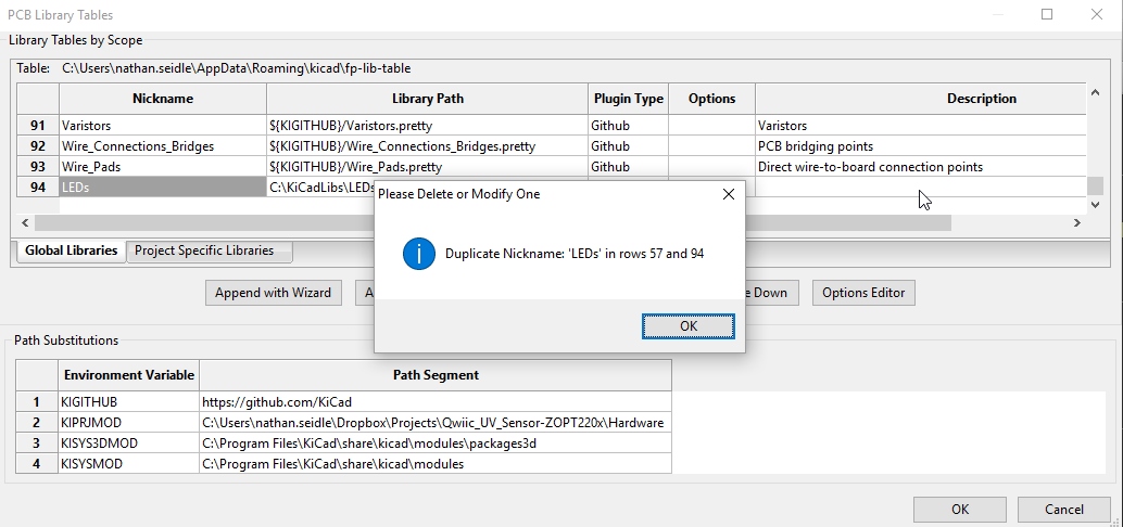
KiCad may throw an error because the 'LEDs' nickname is used twice. I renamed mine to 'LEDs-Custom' then click on 'OK' to close out the Footprint Libraries Manager.
If you inspect the Footprint Editor tool bar again, you'll see the LEDs library is still active and read only. Now we can click on 'File->Set Active Library'. Here is where KiCad shines - the Filter works well. Type LED and select the LEDs-Custom library.
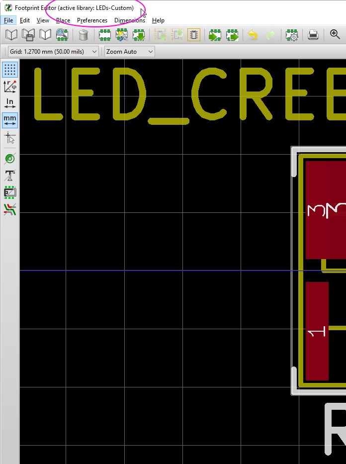
At last! We have an active local library. Now when you click 'Save footprint in local library' or press 'ctrl+s' KiCad will prompt you with a Save Footprint window with Name (annoyingly every time). Press enter and your modifications will be saved.
Now you can explore creating and editing footprints using the Footprint Editor.
After you've created your first footprint or two be sure to read KiCad's KiCad Library Conventions (KLC). It's a well documented system for creating community share-able footprints. Left to our own devices we will all create things a little differently; the KLC tries to get us all on the same page and SparkFun follows it.
In the future, if you're creating a lot of footprints consider using git repo to manage the changes. At SparkFun, we use the following structure:
By using a git repo, SparkFun engineers and our users can contribute schematic components and footprints.
When opening CvPcb to assign footprints to the schematic components, it can take a very long time to load. This is because KiCad is pinging all the KiCad github repos and pulling down 93 libraries. To make this faster, we recommend removing the libraries that are either deprecated or libraries that you will never use.
It's quick and easy to remove a library: select a row in the Footprint Libraries Manager and click the 'Remove Library' button. If something goes wrong, don't panic! Simply click 'Cancel' in the manager window and the library manager will close without saving changes. If things go really wrong, you can always delete the 'fp-lib-table' file and restart KiCad. This will cause it to create the footprint table with the KiCad defaults.
The footprint libraries table file (on Windows 10) is located in your AppData. It should look similar to: 'C:\Users\Nathan\AppData\Roaming\kicad\fp-lib-table' .
Removing the deprecated libraries brings the default count down to 75 and CvPcb still takes an annoyingly long time to load. This is where you'll have to make some tough decisions. Do you plan to ever need the 'Shielding-Cabinets' library? Perhaps. Perhaps not. If I ever do need an RF shield for a design, it will most likely be a custom part or a part that is not in the library. So that one gets the toss.
SparkFun is taking a blended approach. We're becoming very familiar with the default KiCad libraries and using their footprints wherever it makes sense. When we find or use a package we like, we copy it over to the SparkFun-KiCad-Libraries GitHub repo. At the same time, we're continuing to leverage all our custom Eagle footprints that we've been using and creating for over a decade. We know and trust these footprints. I have had many PCBs ruined because I trusted someone else's footprint so I tend to be very paranoid. Use the community where you can but be very rigorous about checking them for correctness.
If you're needing a generic 2x5 pin male header, check the KiCad libraries. It should work fine. However, if you're using a more eclectic part, you may be better off creating the footprint from scratch. Even if the KiCad libraries contain the part, you'll want to check it against the datasheet very closely and do a one to one test print.
If you're familiar with Eagle, it can be scary to think all the time spent creating footprints will be lost when switching to KiCad. Don't fear! KiCad inherently reads Eagle footprints! Yep, it's built right in. Now don't get too excited. KiCad can't read your Eagle schematic components but we have a solution for that in a later section.
The approach we are taking at SparkFun is to link to a local copy of all our classic Eagle Librarie Anytime we need one of the Eagle footprints, we copy and paste it into a modern KiCad library. We don't have to re-create the footprint but by moving it over to a KiCad library. We are able to then edit the footprint as needed. Furthermore, any new footprints are created from scratch and saved to the appropriate SparkFun KiCad library.
You should have already opened the PCB Footprint Editor at least once by now. This will have created a 'fp-lib-table' file that we will be editing shortly. Now to get started, be sure that KiCad is closed.
Download the SparkFun Eagle Libraries from GitHub.
Unzip them into a local directory of your choice. I store our Eagle libraries in a DropBox folder so both my desktop and laptop can access the same set of files.
You could use the Footprint Libraries Manager located in the footprint editor but adding or removing many libraries becomes tedious; it's easier to edit the table file directly.
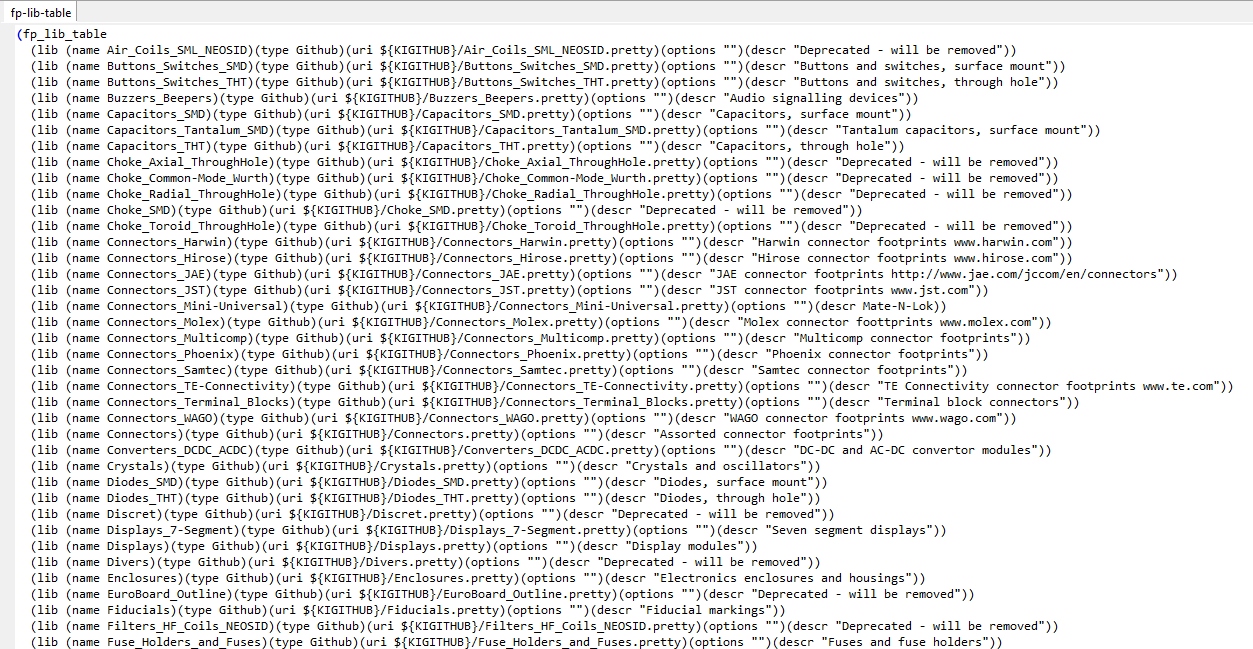
The 'fp-lib-table' tells KiCad where to find all the various libraries and what types of libraries they are (KiCad, github, EAGLE, etc).
We are going to edit this file to add in the SparkFun libraries as well as remove the deprecated libraries and libraries that SparkFun doesn't use.
Here are the files of importance:
Download the 'combined fp-lib-table' to a local folder. Rename it to 'fp-lib-table'. Now move the file to where KiCad expects it. The footprint libraries table file (on Windows 10) is located in the AppData folder similar to: 'C:\Users\Nathan\AppData\Roaming\kicad\fp-lib-table'. You'll want to overwrite the file that is there.
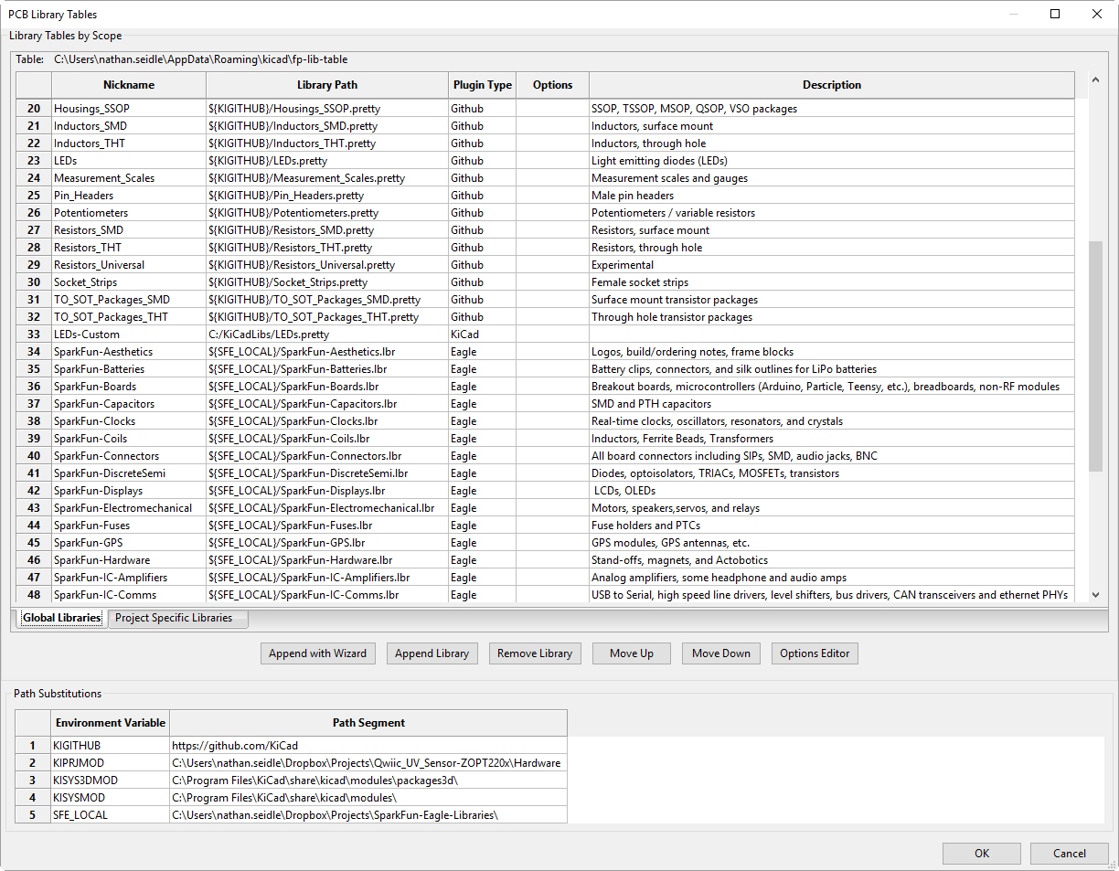
Once the file is in place, re-open KiCad, open the PCB footprint editor, and finally the Footprint Libraries Manager. You should see a long list of libraries including the new SparkFun libraries.
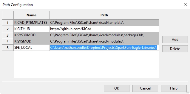
The last step is to tell KiCad the local path to the SparkFun libraries. Currently it's a variable called SFE_LOCAL. We need to assign this to something. Close the Library Manager window, click on Preferences -> Configuration Paths. Click the 'Add' button. Edit the Name and Path fields.
In the image below, you can see I've set the 'SFE_LOCAL' variable to a local path of 'C:\Users\nathan.seidle\Dropbox\Projects\SparkFun-Eagle-Libraries\'. Set this variable to wherever you locally stored the SparkFun Eagle Libraries.
Congratulations! You can now see, use, and copy all the SparkFun Eagle libraries.
Once you've learned to create your own schematic parts and custom footprints, you become unlimited by what technologies you can play with. Let's get started!
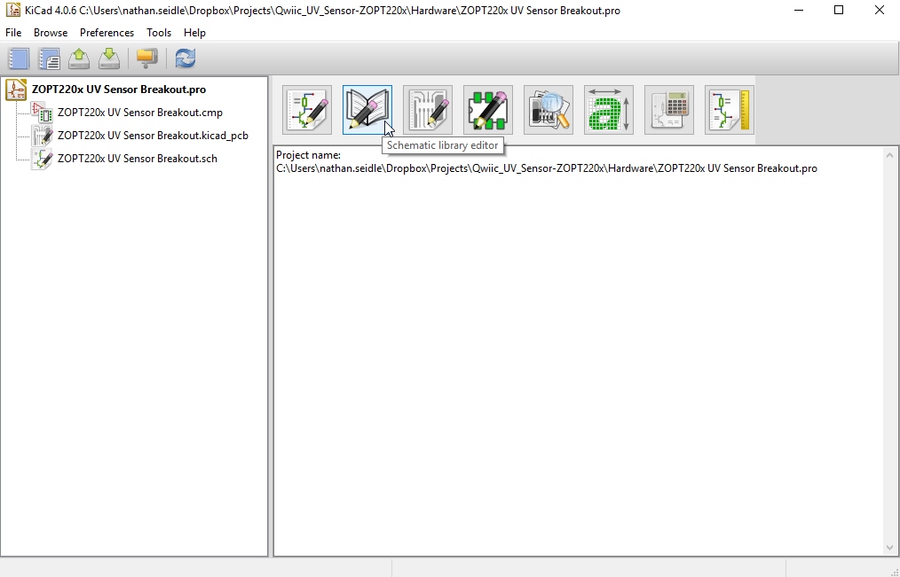
From the main project window start the Schematic library editor.
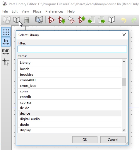
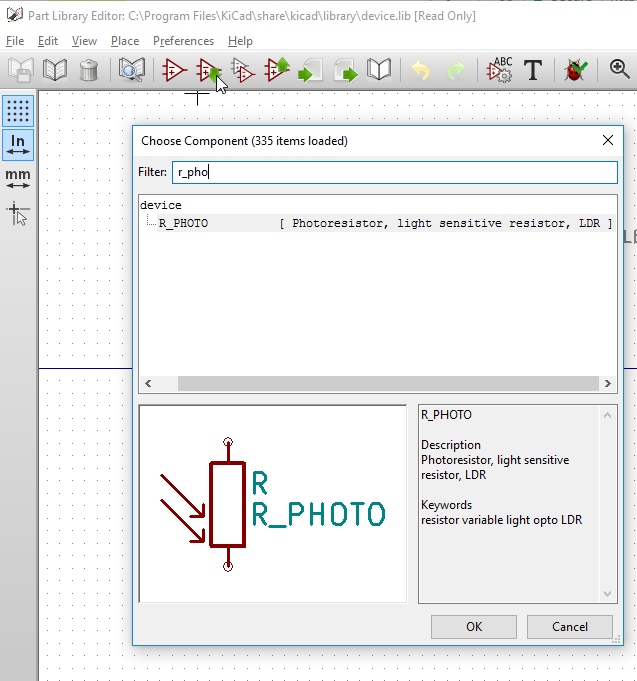
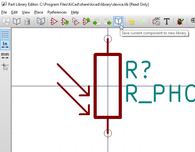
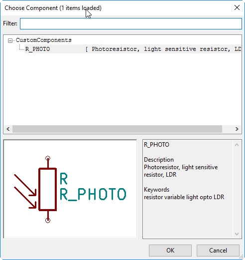
This process is similar to how we started a custom footprint library. First, let's find a schematic symbol we want to start our custom library with. The photocell is just as common as it gets. Let's pull in the 'R_PHOTO' schematic component from the device library and use it to start our new custom schematic component library.
Start by clicking on the 'Selecting working library' (i.e. book) icon located in the upper left corner. Then select 'device' to set the working library.
Click on the 'Load component to edit from current library' button and type r_photo in the filter to quickly locate the photoresistor component. When located, click 'OK'.
Click on 'Save current component to new library' button
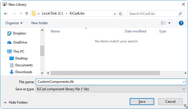
I recommend you store this *.lib file in the same 'C:\KiCadLibs\' directory we stored the footprint library within. I called my lib file 'CustomComponents.lib' so that I know these are mine.
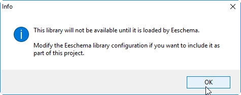
Once you click 'Save', a warning will pop up. This is just KiCad's polite way of letting you know that you can't access your library until you link to it. So let's do that.
Click on Preferences -> Component Libraries to view the current set of libraries. In the image below, we can see the stock schematic component libraries that ship with KiCad. Next to the 'Component library files,' click 'Add'.
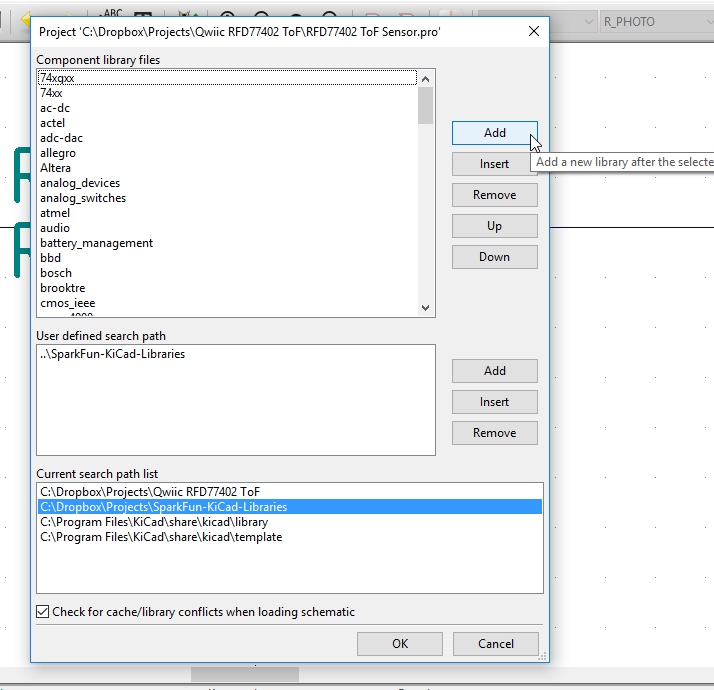
Navigate to your 'C:\KiCadLibs' directory and then open 'CustomComponents.lib'. It should now appear at the bottom of the Component library files list. Click 'OK' to return to the library editor.
Again, click on the 'Select working library' button but this time either scroll to your custom list or type 'Custom' to find the 'CustomComponents' library. Click 'OK'.
Then click on 'Load component to edit from the current library' button and we should see only the photoresistor schematic component. Double click on R_PHOTO to begin editing it.
Now at this point, we can add new symbols from scratch to our library and we can also copy from one library to another.
KiCad is always changing and they've made leaps and bounds improvements but copying a schematic component from one library to another is still a bit wild.
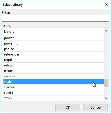
For example, let's copy the CP2104 from the silabs library into our custom library. Start by setting the active library to the one that contains the part you want to copy by clicking on the 'Select working library' button. In our example, we want to set silabs as the active library.
Load the CP2104 component by clicking on the 'Load component to edit from the current library' button.
Now set the active library to the library we want to copy the CP2104 into. For this example, that means that we need to click on the 'Select working library' button and set the active library to 'CustomComponents'.
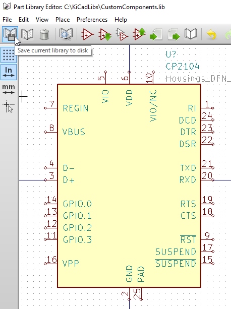
Click on the 'Update current component in current library' button to save the component in CustomComponents.lib. The 'Save current library to disk' button will become enabled and you can save this component to your custom library.
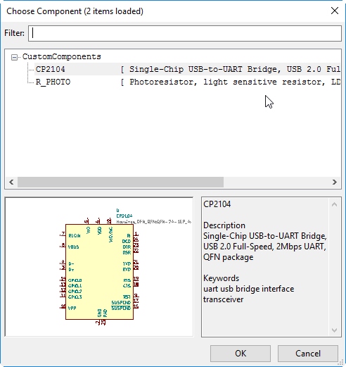
To verify it's now in the library click on the 'Load component to edit from the current library' button. You should see your new shiny CP2104 in the list.
Bad CP2104! Bad component.
To remove a component, be sure you've set your custom library as the active one. Let's try removing the component that we just added in our custom library CustomComponents.lib. If you have not already, click on 'Select working library' to set the active library to CustomComponents. Click on the 'Delete component in current library' (i.e. the trash can) button. You'll be prompted for which component you want to remove. Select CP2104 from the list.
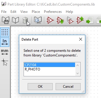
Click 'OK' and then 'Yes' to delete the component from the library. Click the 'Current library to disk' button and 'Yes' to save.
Shout out to Joan_Sparky! He is the best! (No relation)
Be sure to check KiCad's KiCad Library Convention once you get comfortable creating components. These conventions take into account a heap of industry specialized knowledge that we can all benefit from.
Congratulations! That was a big tutorial and you made it through.
For more information related to KiCad, check out the resources below:
Now that you've learned how to modify schematics, PCB layouts, and libraries, it's time to try out your skills on your own custom project. We recommend using the ZOPT220x UV Sensor Breakout KiCad files as the starting point for your next project. From this example project, you can delete or add devices as you need rather than starting from a blank canvas.
Need some more inspiration? Check out SparkFun's Enginursday and project blog posts about KiCad.
If you are an EAGLE guru starting to get your feet wet with KiCad, be sure to checkout Lachlan's Eagle to KiCad converter for converting your Eagle PCB layouts to KiCad. It's not perfect but Lachlan has done a tremendous amount of groundwork.
Thanks for reading and if you have any comments or questions please ask them in the comments section.
Or check out 10-part KiCad video series with Digi-Key and SparkFun as Shawn designs a simple 555 timer circuit for a badge, orders parts, and solders the badge together! The video linked below is just after Digi-Key guides you through KiCad and we begin to apply our skills to create the badge.
learn.sparkfun.com | CC BY-SA 3.0 | SparkFun Electronics | Niwot, Colorado